

Ijraset Journal For Research in Applied Science and Engineering Technology
A Four Element UWB MIMO Antenna with Band - Notched Characteristics for Wireless Communication Applications
Authors: Sharabu Navya, Dr. S. Varadarajan
DOI Link: https://doi.org/10.22214/ijraset.2024.65900
Certificate: View Certificate
Abstract
This study proposes an innovative approach to enhance isolation in a four-element Ultra Wide Band (UWB) range Multiple Input Multiple Output (MIMO) antenna system. The design employs unique rhombic and cross-shaped slot structures to achieve compactness, with dimensions of 34 mm × 34 mm × 1.6 mm. To minimize mutual coupling, the antenna incorporates orthogonally placed feed lines alongside a parasitic strip measuring 17 mm × 1 mm × 1.6 mm. The antenna effectively suppresses interference from specific bands, including WiMAX, WLAN, and X-band, through the integration of L-shaped and C-shaped slits combined with Electromagnetic Band Gap (EBG) elements. Simulation results, verified through practical testing, confirm an operational bandwidth 2 GHz to 12 GHz, excluding the targeted notched bands. The design achieves superior isolation (S11 < -10 dB), a peak gain of 2.5–5 dB, and excellent interference rejection capabilities. These features establish the antenna as a highly efficient option for next-generation UWB-MIMO wireless communication applications.
Introduction
I. INTRODUCTION
The progress in Wireless Communication has leads to the creation of Technologies such as Multiple Input Multiple Output (MIMO) and Ultra Wide Band (UWB), which aim to satisfy the growing need for faster and more efficient data transmission [1]-[2]. MIMO technology is widely acknowledged for its ability to address multipath fading and boost data rates, making it essential for contemporary communication networks. Similarly, UWB technology, known for its extensive frequency range and low power consumption, has diverse applications, including short-range communication, radar, and precise positioning systems [3]-[6]. The combination of MIMO and UWB technologies leverages their unique strengths to enable systems with improved spectral efficiency and greater dependability. However, challenges such as mutual coupling between antenna components and interference with pre-existing communication systems continue to affect system performance, requiring innovative design methodologies to overcome these issues [7]-[12]. To tackle these challenges, the study introduces a Compact UWB MIMO Antenna design. The proposed antenna features a small footprint of 34 mm × 34 mm × 1.6 mm and integrates innovative design elements, including rhombic and cross-shaped slots, parasitic structures, and notched bands. These features contribute to achieving a compact design, improved operational performance, and reduced interference [13]-[17].This study provides a well-researched approach that addresses the key technical challenges faced by UWB-MIMO systems, offering improved performance and reliability for advanced wireless communication applications [18]-[20].
II. ANTENNA DESIGN AND ANALYSIS
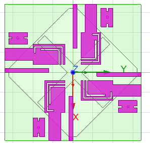
The UWB-MIMO Antenna, as shown in Figure 1, features Measurements of 34 mm × 34 mm × 1.6 mm and is fabricated on a substrate.
Key performance enhancements include:
- Isolation Improvements: Parasitic strips achieve a 4-5 dB reduction in coupling across key frequency ranges.
- Notched Bands: Slits and EBG structures ensure effective suppression of specific interference bands.
- Compact Design: The small footprint supports seamless integration into modern communication systems. The antenna's design consists of four microstrip lines arranged orthogonally to each other, which helps expand the impedance bandwidth at lower frequencies. This configuration also improves, the compact design of the antenna leads to high Mutual Coupling between the Antenna elements.
To improve isolation and mitigate this effect, parasitic strips are strategically placed between the adjacent microstrip-fed lines. This approach effectively reduces Mutual Coupling, improves the overall Performance of the Antenna System.
(a)
(b)
Figure 1 : The Geometry of Proposed UWB MIMO Antenna
- Top Layer, (b) Bottom Layer
Table 1 : Measurements of Parameters for Proposed UWB MIMO Antenna
|
PARAMETER
|
POSITION
|
AXIS
|
|
Substrate
|
(-17 x -17 x 0) mm
|
X=34mm Y=34mm Z=1.6mm
|
|
Microstrip lines (Radiator)
|
(17 x -17 x 1.6) mm
|
X=-7mm Y=3mm
|
|
Parasitic strips
|
(17 x -1 x 1.6) mm
|
X=-11mm Y=1mm
|
|
EBG structure
|
(17 x -10 x 1.6) mm
|
X=-4.6mm Y=2.9mm
|
|
Rhombic slot
|
(-17 x -17 x 0) mm
|
X=34mm Y=34mm
|
|
Cross Shaped Slot
|
(-1 x-11.49 x 0) mm
|
X=2.5mm Y=22.99mm
|
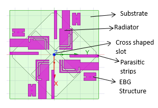
Figure 2: Antenna with name of Parameters
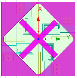
III. DESIGN OF UWB MIMO ANTENNA ELEMENTS
The design features a compact structure that accommodates four microstrip lines arranged orthogonally. This arrangement serves to broaden the impedance bandwidth at lower frequencies and improves the Isolation between the Antenna elements. Although small size of the Antenna could lead to significant mutual coupling, the design includes parasitic strips placed between the adjacent microstrip feed lines to mitigate this issue.
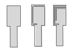
Figure 3: Design of Evolution of Multiple Notched Bands
To improve isolation, additional parasitic strips are placed on top of the substrate between the microstrip lines, supplementing those already located between the microstrip lines. These additional structures act as decoupling elements, leading to a significant reduction in mutual coupling, as shown by the simulated S-parameters. The introduced parasitic strips achieve an isolation improvement of about 5 dB within the 4–6 GHz frequency range and approximately 4 dB within the 5–8 GHz frequency range.
To implement the antenna's triple band-notched behaviour, L-shaped and C-shaped slits are etched into each radiator, and Electromagnetic Bandgap (EBG) structures are strategically positioned near the microstrip feed points. The L-shaped slit is designed to block radiation near the 5.5 GHz frequency, while the C-shaped slit targets radiation at 3.6 GHz.
Additionally, the placement of EBG structures reduces radiation at 8 GHz, contributing further to the antenna's overall performance by mitigating undesired frequency emissions.
Figure 4: EBG Structure
This design approach effectively addresses challenges such as mutual coupling and unwanted radiation, offering enhanced performance in the desired frequency ranges while maintaining a compact antenna footprint suitable for modern communication systems.
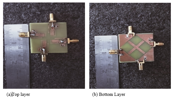
Figure 5: Physical Design of the Proposed Antenna
IV. RESULTS AND DISCUSSION
Thorough testing and simulations were performed to assess the antenna's functionality, leading to significant insights and key results.
A. S-PARAMETERS:
S-Parameters or Scattering Parameters are a tool used to evaluate the performance of Antennas and Electronic Systems. S-Parameters are a set of interconnected measurement that describe how waves reflect in a Network.
S-Parameters help Engineers to understand how efficiently Antennas Radiate or Receive Electromagnetic Waves and how well they matched with a Transmission line.
They can also be used to optimize Antenna designs to achieve Desired Radiation Patterns. S-parameters are a method of representing systems using general wave quantities rather than voltages and currents. The S_11 is also known as the Reflection Coefficient.
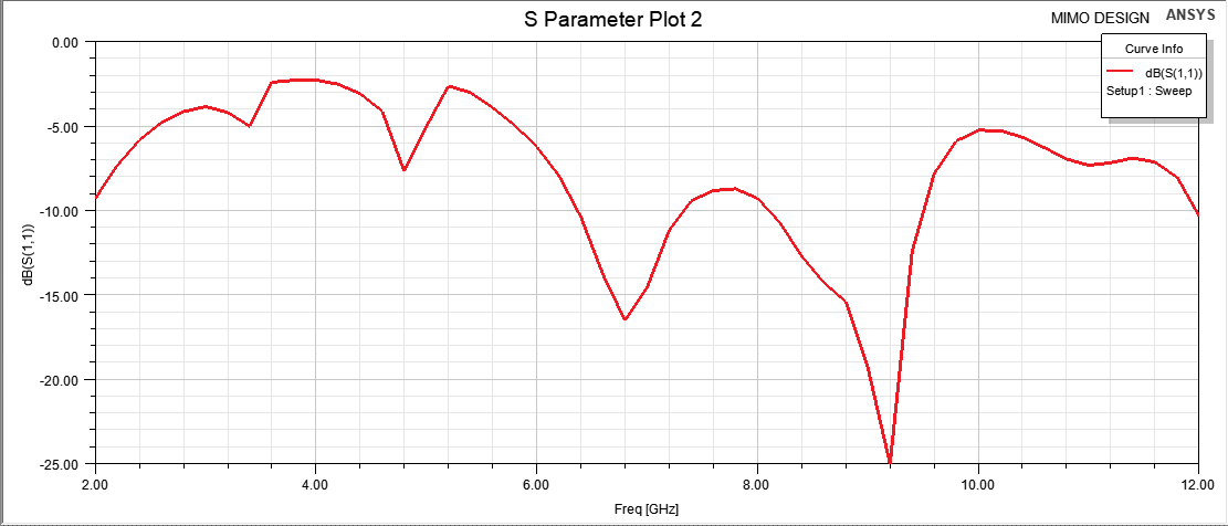
Figure 6: Simulated S11 Parameter
S_11 related to Return Loss. It describes how the waves are Radiated or Transmitted from/through the device.

Figure 7: Measured S11 Parameter
In an Antenna, S-Parameters S13, S23, S24, S22 can be Related to Signal Transmission and Reflection measurements.
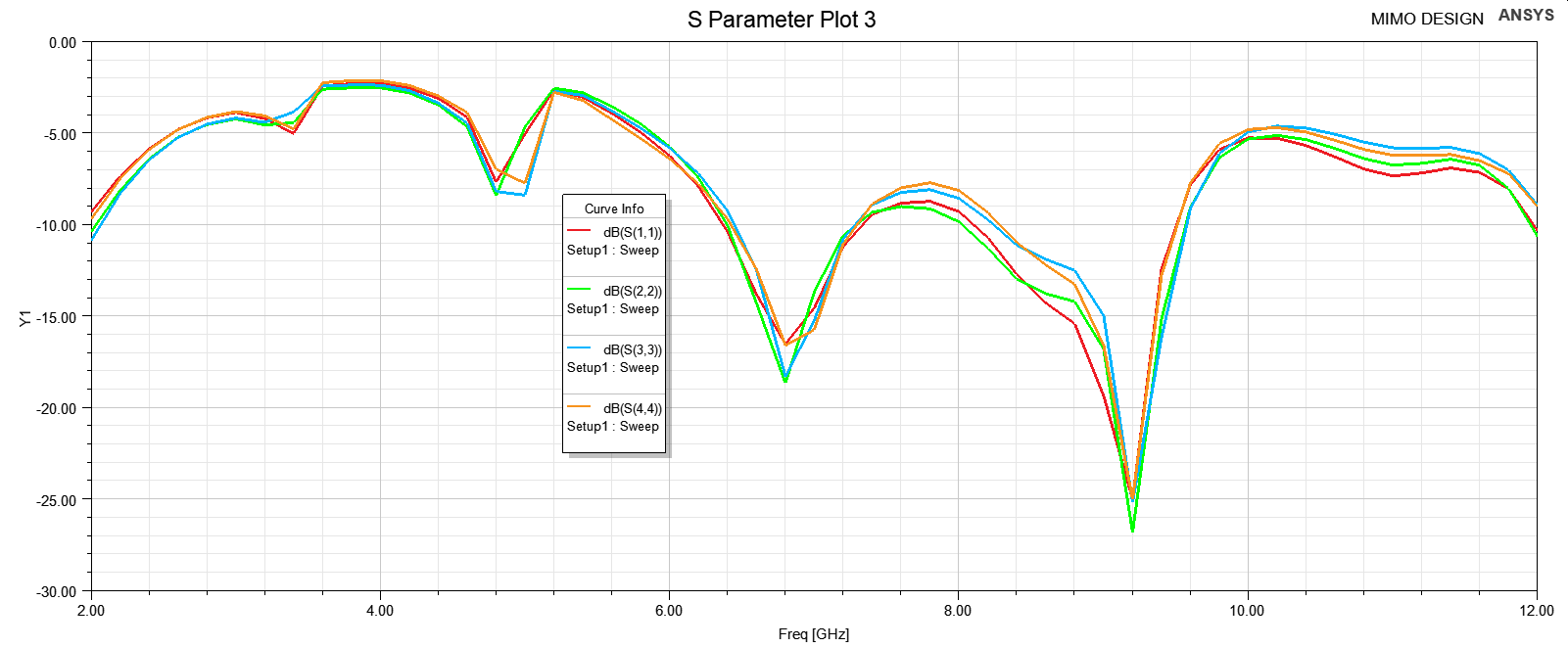
Figure 8: Simulated S-Parameters S11, S22, S33
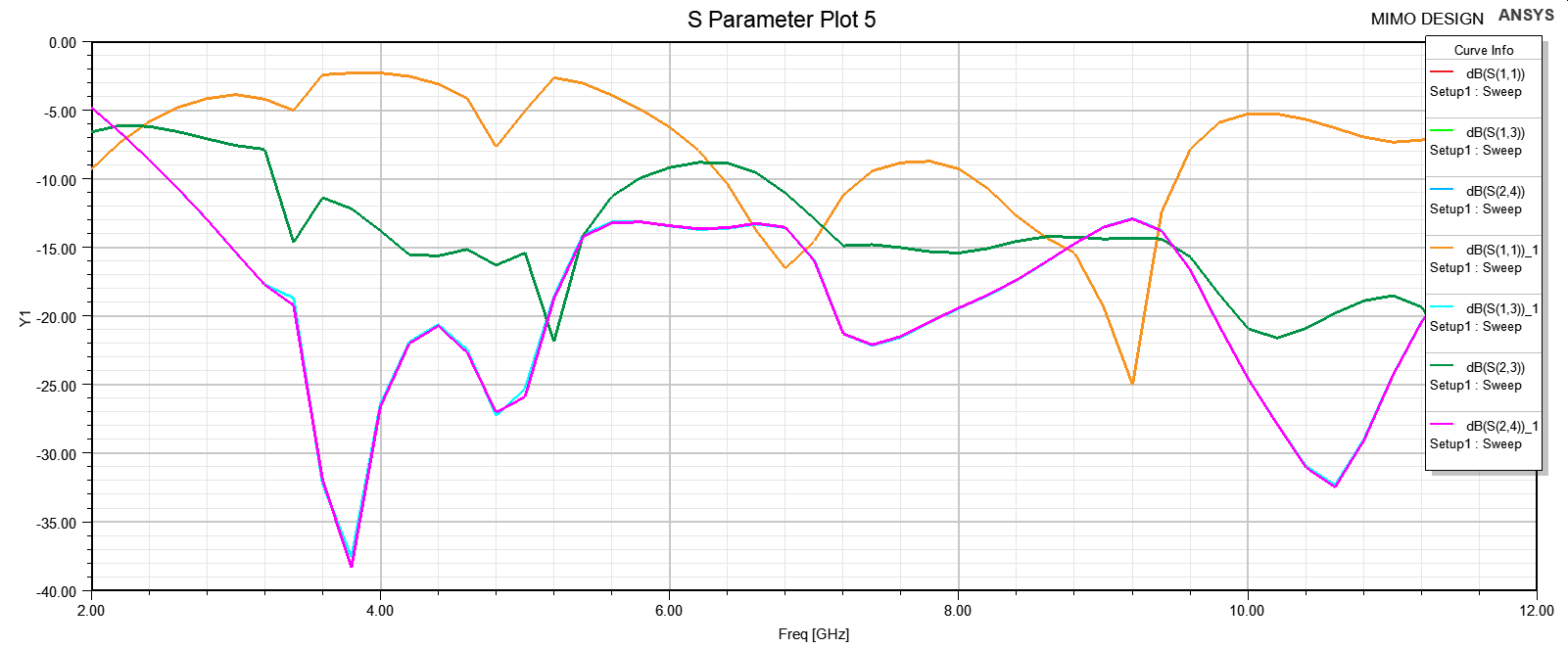
Figure 9: Simulation of S-Parameters S11, S13, S22, S23, S24
Table 2.1 : S Parameters Values

Table 2.2 : S Parameters Values
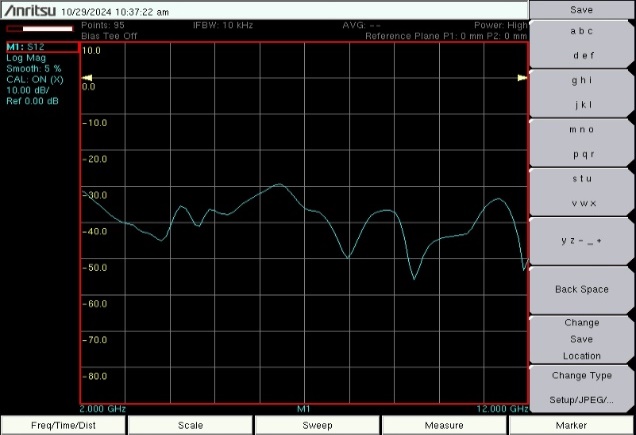
Figure 10: Measured S13 Parameter
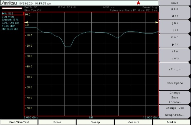
Figure 11: Measured S22 Parameter

Figure 12: Measured S23 Parameter
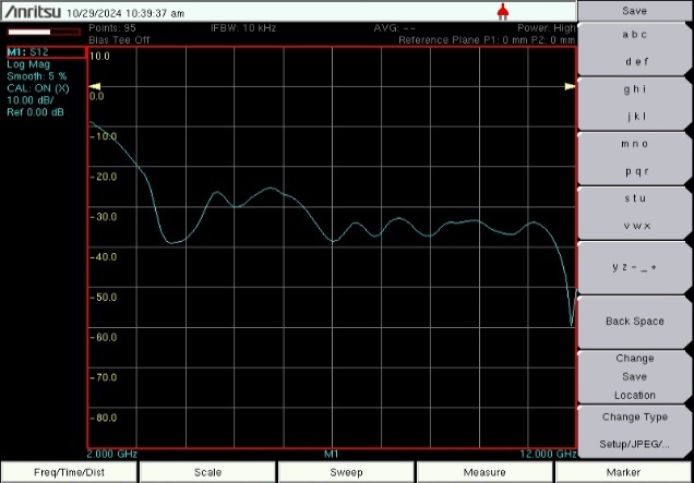
Figure 13: Measured S24 Parameter
S13 and S23 are Scattering coefficients, these are equal if the junction is symmetrical in plane ,S11or S22 indicates a signal reflection measurement.S21or S12 indicate Transmission measurements.
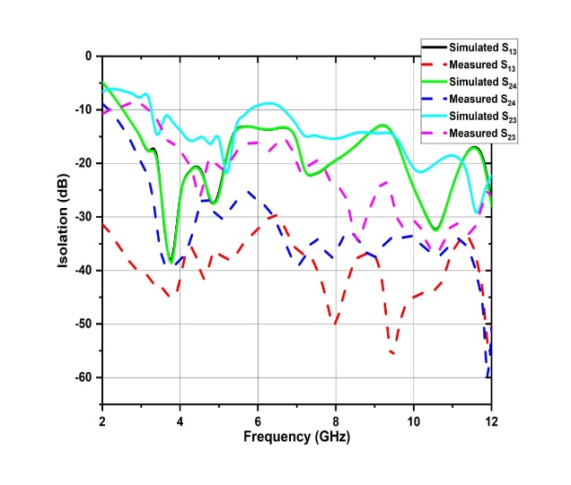
Figure 14: Simulated & Measured S-Parameters
B. SMITH CHART:
The Smith Chart is utilized to represent the antenna's impedance across varying frequencies, facilitating efficient impedance matching.
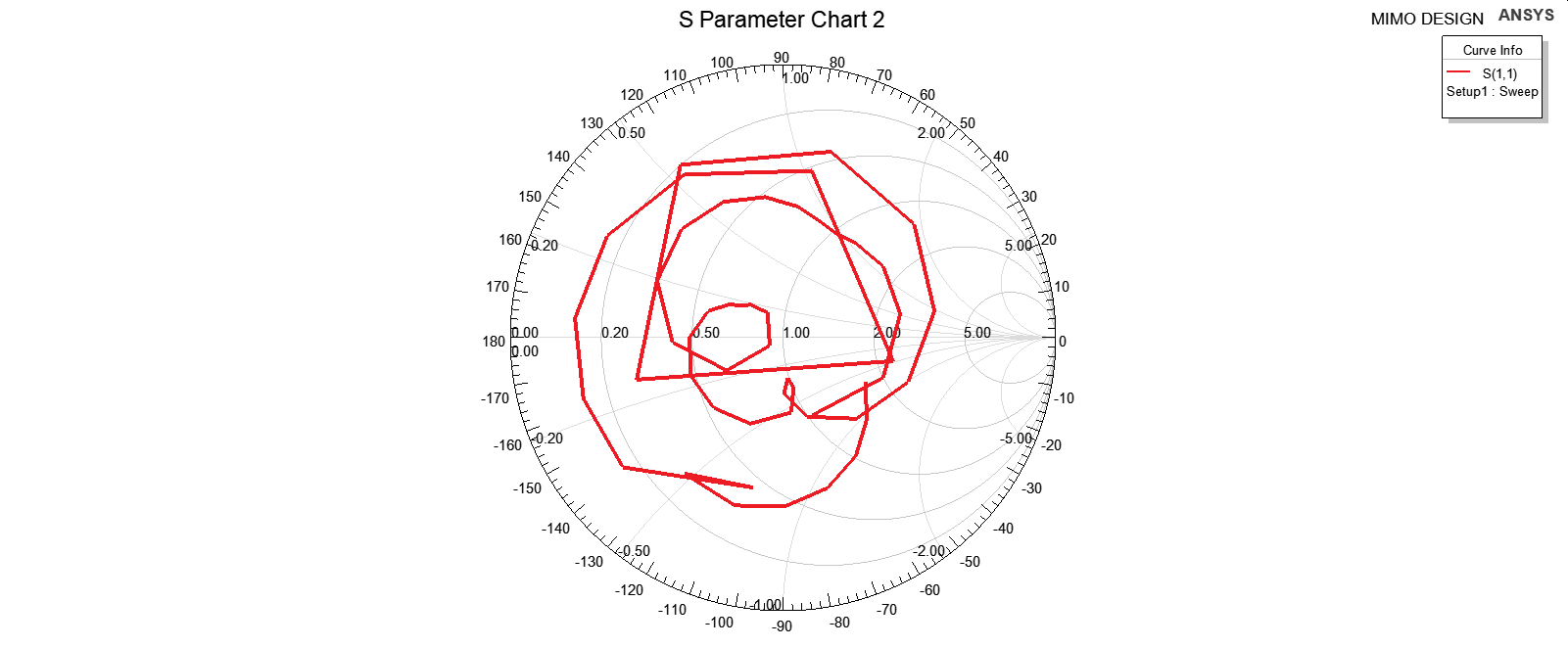
Figure 15: Simulated of Smith Chart
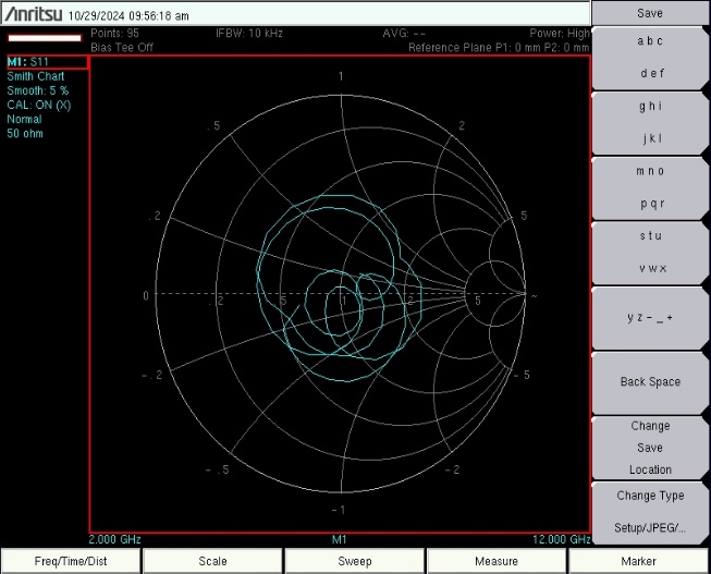
Figure 16: Measured Smith Chart of Antenna
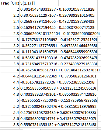
Table 3.1: Smith Chart Values
The Smith Chart is instrumental in achieving the desired frequency response characteristics by adjusting component values and performing impedance transformations.
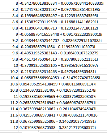
Table 3.2: Smith Chart Values
C. VSWR
The Voltage Standing Wave Ratio (VSWR) remains below, ensuring minimal reflection and maximum signal transfer.
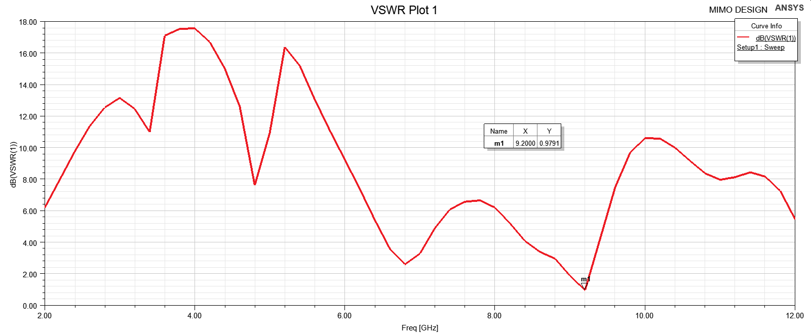
Figure 17: Simulated VSWR of Antenna
The Voltage Standing Wave Ratio (VSWR) is a vital parameter that evaluates the alignment of impedance between an antenna and a transmission line, providing insight into the effectiveness of power transfer.

Figure 18: Measured VSWR of Antenna
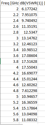
Table 4.1: VSWR Values
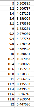
Table 4.2: VSWR Values
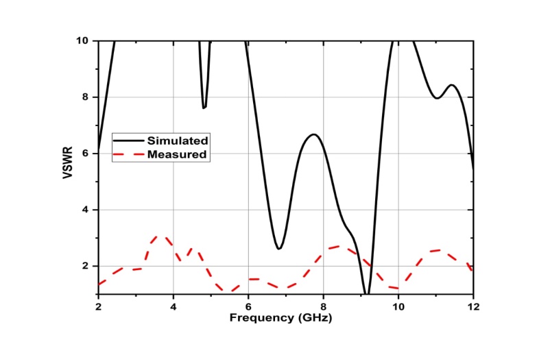
Figure 19: Simulated & Tested VSWR of Antenna
D. IMPEDANCE(Z-PARAMETER):
Antenna impedance consists of two parts: the real part, known as resistance, and the imaginary part, called reactance.
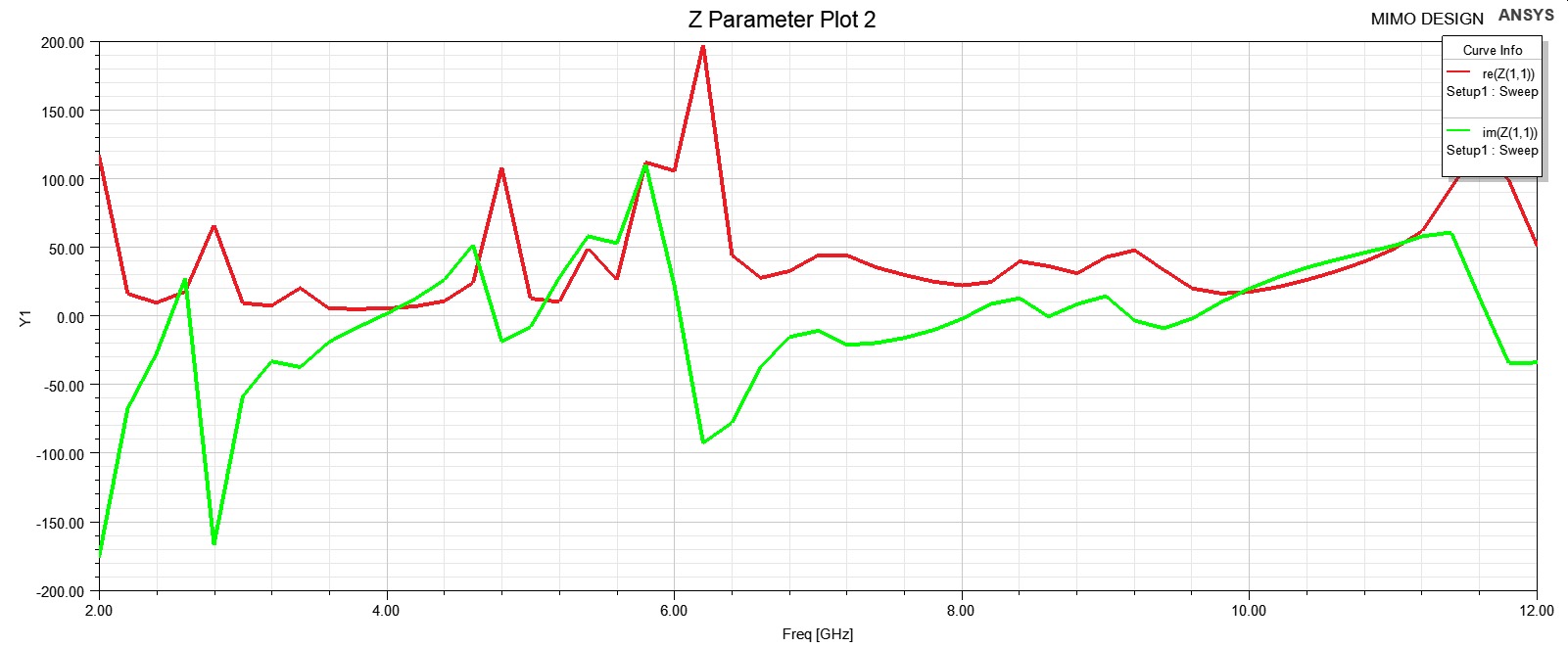 Figure 20: Simulated Impedance of Antenna
E. IMPEDANCE REAL PART:
The real component of the antenna's impedance represents the power that is either emitted as radiation or absorbed by the antenna itself.
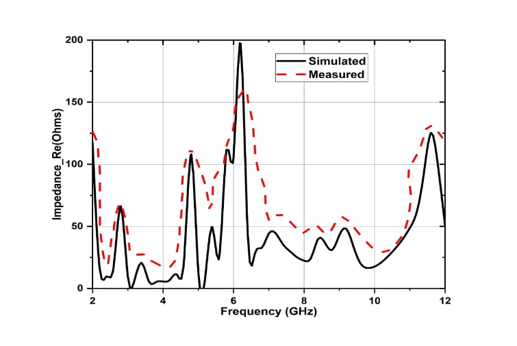
Figure 21: Simulated & Tested real part of Antenna
F. IMPEDANCE IMAGINARY PART:
The Imaginary Part of impedance corresponds to the power stored within the antenna's near-field area.
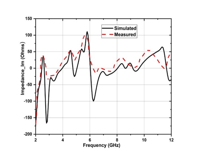
Figure 22: Simulated & Tested Imaginary part of Antenna
G. GAIN:
The Antenna provides a Gain between 2.5 to 5 dB over its operational bandwidth, with consistently high radiation efficiency maintained across the entire range.

Figure 23: Gain of Antenna
These results highlight the antenna’s capability to deliver reliable performance, high isolation, and efficient signal transmission for modern UWB-MIMO systems.
Conclusion
This study introduces a unique UWB-MIMO antenna design that effectively tackles challenges related to size, mutual coupling, and interference in wireless communication technologies. The proposed antenna covers an extensive operational frequency varies from 2 GHz to 12 GHz while maintaining excellent isolation and effectively reducing interference from WiMAX, WLAN, and X-band signals. Key design advancements, such as the inclusion of parasitic strips, specialized notched filters, and innovative slot shapes, play a significant role in achieving the antenna\'s high performance. Both simulation and experimental testing have confirmed the design\'s effectiveness, demonstrating its potential for practical deployment in real-world wireless communication scenarios. For future work, research efforts can focus on enhancing the antenna’s functionality by incorporating reconfigurable elements or developing even smaller, more versatile designs to address the evolving requirements of wireless communication systems.
References
[1] T. Hemalatha and Bappadittya Roy, “Low Profile CO-CSRR and EBG Loaded Tri-Quarter Circular Patch EWB MIMO Antenna with Multiple Notch Bands”, IEEE open journal of Antennas and Propagation, vol.5, N0.3, June 2024. [2] ZHIJIAN CHEN, WEISI ZHOU, AND JINGSONG HONG,”A Miniaturized MIMO Antenna With Triple Band-Notched Characteristics for UWB Application”,DOI:10.1109/ACCESS.2021.307451 [3] M. G. N. Alsath and M. Kanagasabai, “Compact UWB monopole antenna for automotive communications”, IEEE Trans. Antennas Propag., vol. 63, no. 9, pp. 42044208, Sep. 2015. [4] E. M. Staderini, “UWB radars in medicine”, IEEE Aerosp. Electron. Syst. Mag., vol. 17, no. 1, pp. 1318, Jan. 2002. [5] J. Zhang, P. V. Orlik, Z. Sahinoglu, A. F. Molisch, and P. Kinney, “UWB systems for wireless sensor networks”, Proc. IEEE, vol. 97, no. 2, pp. 313331, Feb. 2009. [6] B. Sobhani, E. Paolini, A. Giorgetti, M. Mazzotti, and M. Chiani, “Target tracking for UWB Multistatic radar sensor networks”, IEEE J. Sel. Topics Signal Process., vol. 8, no. 1, pp. 125136, Feb. 2014. [7] R. Kshetrimayum, “An introduction to UWB communication systems”, IEEE Potentials, vol. 28, no. 2, pp. 913, Mar./Apr. 2009. [8] C. King, “Fundamentals of wireless communications”, presented at the 67th Annu. Conf. Protective Relay Eng., College Station, TX, USA, 2014. [9] M. Weisenhorn and W. Hirt, “Performance of binary antipodal signal over indoor UWB MIMO Channel”, presented at the IEEE Int. Conf. Commun., Anchorage, AK, USA, 2003. [10] M. Bilal, R. Saleem, H. H. Abbasi, M. F. Sha que, and A. K. Brown, “An FSS-based nonplanar quad-element UWB-MIMO antenna system”, IEEE Antennas Wireless Propag. Lett., vol. 16, pp. 987990, 2017. [11] X. Zhao, S. P. Yeo, and L. C. Ong, “Planar UWB MIMO antenna with pattern diversity and isolation improvement for mobile platform based on the theory of characteristic modes”, IEEE Trans. Antennas Propag., vol. 66, no. 1, pp. 420425, Jan. 2018. [12] G. Irene and A. Rajesh, “A dual-polarized UWBMIMO antenna with IEEE 802.11ac band-notched characteristics using split-ring resonator”, J. Comput. Electron., vol. 17, no. 3, pp. 10901098, Sep. 2018. [13] S. Rajkumar, K. T. Selvan, and P. H. Rao, “Compact 4 element sierpinski knopp fractal UWB MIMO antenna with dual band notch”, Microw. Opt. Technol. Lett., vol. 60, no. 4, pp. 10231030, Apr. 2018. [14] S. Das, P. Chowdhury, A. Biswas, P. P. Sarkar, and S. K. Chowdhury, “Analysis of a miniaturized multi resonant wideband slotted microstrip antenna with modified ground plane”, IEEE Antennas Wireless Propag. Lett., vol. 14, pp. 6063, 2015. [15] R Zhen, X. Zhang and H. Zheng, “A Compact MIMO antenna with two band-notches for Mobile Devices”,2023 IEEE 6th International Conference on Electronic Information and Communication Technology (ICEICT), Qingdao, China, pp. 922-925. [16] S. B. Paiva, J. G. D. Oliveira, J. K. A. Nogueira, V. P. S. Neto,” A Miniaturized MIMO Antenna with Band-Notched Characteristic for UWB Applications”2023 IEEE MTT-S International Microwave and Optoelectronics Conference (IMOC), Spain, pp. 172-174. [17] S. Koziel and M. A. UI Haq, “Ground plane modifications for design of miniaturized UWB Antenna”, 2018 DOI: 10.1049/iet-map.2017.1111 [18] Y. Ye, X. Zhao and J. Wang, “Compact High-Isolated MIMO Antenna Module with Chip Capacitive Decoupler for 5G Mobile Terminals”, 2022 IEEE Antennas and Wireless Propagation Letters, vol. 21, no. 5, pp. 928-932 [19] G. Srivastava, A. Mohan and A. Chakrabarty Compact reconfigurable UWB slot Antenna for cognitive Radio Application”,2017 DOI: 10.1109/LAWP.2016.2624736, IEEE. [20] A. Iqbal, A. W. Ahmad and S. Bashir, “Mutual coupling reduction using f-shaped stubs in UWB MIMOAntenna”,2018DOI:10.1109/ACCESS.2017.2785232.
Copyright
Copyright © 2024 Sharabu Navya, Dr. S. Varadarajan. This is an open access article distributed under the Creative Commons Attribution License, which permits unrestricted use, distribution, and reproduction in any medium, provided the original work is properly cited.

Download Paper
Paper Id : IJRASET65900
Publish Date : 2024-12-13
ISSN : 2321-9653
Publisher Name : IJRASET
DOI Link : Click Here
 Submit Paper Online