

Ijraset Journal For Research in Applied Science and Engineering Technology
An Area and Power Optimization for Level Shifters using 45nm CMOS Technology
Authors: Harshitha B, Nayana V S
DOI Link: https://doi.org/10.22214/ijraset.2024.62674
Certificate: View Certificate
Abstract
Modern integrated circuits require level shifters as essential parts to enable communication between circuits running at various voltage levels. Design-wise, the Level Shifter has a minimal silicon footprint due to its limited component count and operates with minimal power usage, making it well-suited for energy-efficient applications. This work implements CMOS voltage level shifter, also known as conventional CMOS level shifter. The level shifter\'s overall power and area usage are compared. CMOS level shifters simulations are carried out using CADENCE tool. The simulation\'s outcomes are implemented in conventional 45-µm CMOS technology.
Introduction
I. INTRODUCTION
With the escalating demand for portable electronic gadgets like iPods, cameras, and cell phones is growing daily, system design must take low power consumption into consideration. In VLSI circuits, there exist two categories for imperativeness dispersal: dynamic and static power dispersal. The immediate result of the store capacitor being charged and released is dynamic power distribution. Static power dispersal is occurred by spilled current flowing across VLSI circuitry. The primary cause of dissipation of electricity is the supply voltage. Therefore, by adjusting the supply voltage, the overall power dissipation can be decreased. Leakage current, a minor voltage fluctuation, and insufficient noise margin are all effected by the supply voltage drop. Reducing the entire power dissipation also results in a decrease in the device dimensions, although caution should be used when reducing them because, even at low supply voltage, device breakdown may happen if the dimensions are lowered below a specific point. Thus, by taking a theoretical approach into consideration, gadget dimensions should decrease.
There are two varieties: low-level shifters and high-level shifters. Because some devices might need a high voltage to turn on, a high-level shifter is needed to move the voltage levels from low to high. Like high- level shifters, low-level shifters are employed to transform the voltage from a high to a low level because some devices might need a low voltage to operate. In the literature, different designs for level shifters with single and dual supply voltages have been documented.
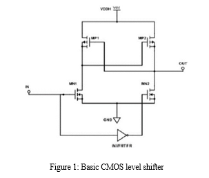
In Figure 1, a basic CMOS LS is displayed. Two NMOS transistors, MN1 and MN2, and two PMOS transistors, MP1 and MP2, make up this arrangement. An inverted output of MN1 is provided to MN2. VDDH is one voltage source. In digital electronics, a level shifter—also referred to as a voltage level translator or a logic-level shifter—is a circuit that converts signals between one logic level and one voltage domain (VDD/VSS). It makes it possible for various sub-chip blocks of integrated circuits (ICs) with various voltage requirements to work together, including complementary metal-oxide-semiconductor (CMOS) and transistor-transistor logic (TTL). In contemporary systems, LS are employed to connect different domains, including processors, logic units, sensors, and various circuits. In VLSI, the prevailing logic voltage levels typically include 1.8V, 3.3V, and 5V. However, levels above and below these voltages are also used. If voltage levels are far apart, the LS design becomes complex and error prone. This design approach is typically found in medium- speed systems and applications, including WSN, miniature healthcare devices, and systems for atmospheric surveillance. Many LS are designed and implemented using different technologies.
II. LITERATURE SURVEY
Here is a detailed summary of some of the existing research studies on this topic:
- S. Kabirpour and M. Jalali (2019) proposed in their research paper titled "A Low-Power and High-Speed Voltage Level Shifter Based on a Regulated Cross-Coupled Pull- Up Network," the enhancement in switching performance and substantial reduction in power consumed dynamically are achieved by incorporating a pull- up network for regulated cross-coupled. The primary objective of the LS is to efficiently convert signals from, the deep subthreshold range to higher and standard supply voltages. Post-layout simulations illustrate the efficacy of the modulated cross-coupled pull-up network, with a comparative analysis against prior research in a 0.18-µm CMOS technology. The LS exhibits a power dissipation of 123.1nW and a propagation delay of 23.7 ns for an input frequency of 1 MHz and a low/high supply voltage of 0.4/1.8 V.
- V. L. Le and T. T. Kim (2018), present in their research paper titled "An Area and Energy Efficient Ultra-Low Voltage Level Shifter With Pass Transistor and Reduced-Swing Output Buffer in 65-nm CMOS," Level Shifter delivers superior performance and enhanced energy efficiency by specifically addressing reduced swing. It instigates a novel reduced-swing buffer design to minimize standby power consumption, while incorporating a pass transistor to boost the celerity of the falling transition. This innovative LS demonstrates notable improvements, with a 16.3× reduction in leakage and a 2.7× increase in speed in contrast to the WCMLS. Furthermore, it achieves a significant 8.5× reduction in switching energy and can efficiently convert voltages from as low as 100 mV in the deep subthreshold range to a super-threshold voltage of 1.2 V.
- In their survey paper titled "A Compact 31.47 fJ/Conversion Subthreshold Level Shifter With Wide Conversion Range in 65 nm MTCMOS," Y. Cao, B. Wang, X. Pan, X. Zhao, Z. Wen and A. Bermak (2018), a front-end current mirror and an output cross-coupled structure. The prototype was fabricated using a commercial 65nm CMOS process. Experiments show that a 90mV low input voltage can be successfully converted to 1.2V. The energy consumed per conversion is reputed to be 31.47fJ for converting a 0.2V input to 1.2V at 10MHz, and the corresponding propagation delay is measured to be 23.98ns.
- Badal, Mohammad Torikul Islam et al. (2017) in their research paper titled “Design of a Low-power CMOS Level Shifter for Low-delay SoCs in Silterra 0.13 µm CMOS Process.” Low power dissipation and low delay are the main design considerations for high performance LS. The presented LS is designed to take input signal of 1 V and convert that into an output signal of 1.8 V which is simulated in Silterra 0.13 µm CMOS process. As claimed by the post-layout simulation results, the intended LS circuit has a notable low power dissipation of only 0.1449nW and low output delay of 25.55ps covering only 17.36× 14.560 µm2 chip area.
- Z. Yong, X. Xiang, C. Chen and J. Meng (2017) in their research paper titled as "An Energy-Efficient and Wide-Range Voltage Level Shifter With Dual Current Mirror," Dual current mirror (CM) configuration, comprising a virtual CM and an auxiliary CM, is put forward to achieve a wide range of conversion. The circuit has been fabricated and fine-tuned using SMIC's 40-nm technology. Post-layout simulations result with LS which can efficiently convert voltages from 0.2 to 1.1 V. Notably, at the target voltage of 0.3 V, the proposed LS demonstrates an average propagation delay of 66.48 ns, a total energy consumption per transition of 72.31 fJ, and a static power draw of 88.4 PW. These results represent significant enhancements of 6.0×, 13.1×, and 89.0×, respectively, in contrast to a Wilson CM-based LS.
- K. Patkar and S. Akashe (2016) in their research paper titled as "Design of level shifter for low power applications," to design a conventional level shifter, six, eight, and ten transistors are being used. Average noise, average power dissipation, and leakage voltage are the parameters being computed for the circuit design. Between 0.2 and 0.7 volts have been the voltages utilized to keep the designed circuits operating. An extremely low voltage input can be handled by a conventional level shifter. For ICs and system-on-a-chip (SoC), this level shifter will be helpful in meeting the requirements of lower power systems.
III. PROBLEM STATEMENT
Level shifter designs should be able to achieve the desired functionality while occupying a minimum area on the integrated circuit. This is particularly important as the technology node progresses to smaller sizes, such as 45nm CMOS. Level shifters should consume minimal power during operation to maintain overall power efficiency of the integrated circuit.
IV. PROPOSED METHODOLOGY
An intelligent mapping mechanism between the IC symbol terminals and the footprint terminals can be created using the Virtuoso System Design Platform. In cases where a schematic symbol is not present, it allows binding to a sub-circuit model of the IC. So, the Conventional CMOS Level Shifter is simulated using 45nm CMOS technology with CADENCE tool.
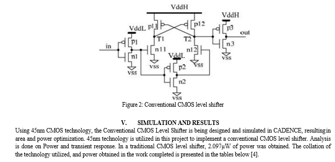
A. Conventional CMOS Level Shifter
The conventional level shifter, as represented in Figure 1, employs cross- coupled PMOS loads. To handle high voltage stress, thick gate oxide transistors (MN11, MN12, MP11, and MP12) are utilized. MN11 and MN12 control the gate-source voltage, which, in turn, affects the latching voltage at nodes T1 and T2. This latching voltage plays a key role in facilitating a positive feedback mechanism involving cross- coupled MP11 and MP12, ultimately resulting in a fully VddH voltage at node T1. When VA is at a low state, MN11 and MP12 are turned on, while MN12 and MP11 are OFF. If VA transitions to a high state, the following sequence of events occurs: MN11 turns off, MN12 turns on, MP11 turns on, causing node T1 to switch from a low to a high state, and MP12 turns off. The time it takes for this transition from a low voltage to a high voltage is determined bythe current driving ability of MP11. Pull-down n-mos must overcome the PMOS latch action before the output change state, so the size of MN11 and MN12 are much larger than MP11, MP12.
Conventional CMOS (Complementary Metal-Oxide-Semiconductor) level shifters offer several notable advantages when it comes to interfacing signals involving various voltage domains within integrated circuits. Firstly, their notable qualities include low power , making them ideal for energy-efficient and battery-powered devices. Furthermore, integration into current chip designs and manufacturing workflows is made easier by their compatibility with standard CMOS processes. Their high-speed operation, compact size, and minimal leakage current make them suitable for an extensive scale of applications. Moreover, CMOS level shifters exhibit robustness across varying environmental conditions, and their scalability and versatility make them adaptable to different voltage levels and performance requirements. Furthermore, they are cost-effective to manufacture owing to the widespread use of CMOS technology in the semiconductor industry, making them a practical choice for high-volume production. Overall, CMOS level shifters are reliable, efficient, and versatile components essential for modern integrated circuit designs.
Conclusion
The amount of power and area is optimized in the Conventional CMOS level shifter is compared and analyzed. Also, layout for the Conventional CMOS level shifters is designed. The LS circuit is reported in this work to meet the prerequisite t of low power consumption. VLSI layout of LS has been designed and checked with Layout Versus Schematic (LVS) checking and concluded that layout design matches the schematic design. Moreover, the designed circuit has managed to achieve significant low power of 2.097 µW. By achieving area and power optimization, the efficiency and cost- effectiveness of level shifter designs in 45nm CMOS technology, which may have an impact on the overall performance of the IC, power usage, and chip area utilization.
References
[1] S. Kabirpour and M. Jalali, \"A Low-Power and High-Speed Voltage Level Shifter Based on a Regulated Cross-Coupled Pull- Up Network,\" in IEEE Transactions on Circuits and Systems II: Express Briefs, vol. 66, no. 6, pp. 909-913, June 2019, doi: 10.1109/TCSII.2018.2872814. [2] V. L. Le and T. T. Kim, \"An Area and Energy Efficient Ultra-Low Voltage Level Shifter With Pass Transistor and Reduced-Swing Output Buffer in 65-nm CMOS,\" in IEEE Transactions on Circuits and Systems II: Express Briefs, vol. 65, no. 5, pp. 607- 611, May 2018, doi: 10.1109/TCSII.2018.2820155. [3] Y. Cao, B. Wang, X. Pan, X. Zhao, Z. Wen and A. Bermak, \"A Compact 31.47 fJ/Conversion Subthreshold Level Shifter With Wide Conversion Range in 65 nm MTCMOS,\" in IEEE Access, vol. 6, pp. 54976-54981, 2018, doi: 10.1109/ACCESS.2018.2871187. [4] Badal, Mohammad Torikul Islam et al. “Design of a Low-power CMOS Level Shifter for Low-delay SoCs in Silterra 0.13 µm CMOS Process.” Journal of Engineering Science and Technology Review 10 (2017): 10-15 [5] Z. Yong, X. Xiang, C. Chen and J. Meng, \"An Energy-Efficient and Wide-Range Voltage Level Shifter With Dual Current Mirror,\" in IEEE Transactions on Very Large Scale Integration (VLSI) Systems, vol. 25, no. 12, pp. 3534-3538, Dec. 2017, doi: 10.1109/TVLSI.2017.2748228. [6] K. Patkar and S. Akashe, \"Design of level shifter for low power applications,\" 2016 Symposium on Colossal Data Analysis and Networking (CDAN), Indore, India, 2016, pp. 1-4, doi: 10.1109/CDAN.2016.7570905.
Copyright
Copyright © 2024 Harshitha B, Nayana V S. This is an open access article distributed under the Creative Commons Attribution License, which permits unrestricted use, distribution, and reproduction in any medium, provided the original work is properly cited.

Download Paper
Paper Id : IJRASET62674
Publish Date : 2024-05-24
ISSN : 2321-9653
Publisher Name : IJRASET
DOI Link : Click Here
 Submit Paper Online