Ijraset Journal For Research in Applied Science and Engineering Technology
- Home / Ijraset
- On This Page
- Abstract
- Introduction
- Conclusion
- References
- Copyright
Implementation and Analysis of CMOS and Pass Transistor Logic Based Full Adder Circuits
Authors: J Rajitha, G Mahesh Babu, K Kavya, K Navina, T Tharun Teja, G Sujatha
DOI Link: https://doi.org/10.22214/ijraset.2024.58495
Certificate: View Certificate
Abstract
In electronic industry the level of integration is an important aspect as it makes the electronic device simpler and more reliable. The device density increases with the better level of integration. Power dissipation, Area occupied and Propagation delay are some of the important factors that need to be considered. These parameters play a vital role in manufacturing portable electronic gadgets. Many binary adders are formed using full adders. Hence, if any enhancements have to be made to improve the performance, it can be made at the root level i.e., adders circuits itself. This in turn helps in bettering the performance of the electronics circuits which follow adder circuits. The low power VLSI design is of great importance due to portable electronic products. Full adder is a type of adder circuit that adds three inputs and gives two outputs. Out of three, two will be the present inputs and the third input will be the carry from the previous stage. ‘A’ and ‘B’ are the actual inputs, ‘C’ is the carry from the previous operation. SUM and CARRY OUT are the two outputs. In this work, Design and Implementation of full adder using conventional CMOS design and Pass Transistor Logic based Full adder circuits are carried out. At last comparison is made between the two designs with respect to power dissipation, delay and area (number of transistors). Cadence Virtuoso Tool is used in design and simulation conventional CMOS design and Pass Transistor Logic based Full adder circuits. The entire work is simulated in 180nm CMOS technology.
Introduction
I. INTRODUCTION
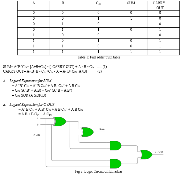
The full adder is generally is used as a component in a cascade of adders where the circuit performs the arithmetic sum of eight, sixteen or thirty two bit binary numbers. Digital Systems performs a variety of operations. Among various information processing tasks are the arithmetic operations which includes binary addition, subtraction, multiplication and division[1]. The most common and basic arithmetic operation is addition of two binary digits. The simplest digital circuit which performs the binary addition operation on two binary digits is called Half Adder[2]. The addition of three binary digits is performed by Full Adder. A Full Adder is the digital Circuit which implements addition operation on three binary digits[3]. Two of the three binary digits are significant digits A and B and one is the carry input (C-IN) bit carried from the previous-less significant stage[4]. Thus the Full Adder operates on these three binary digits to generate two binary digits at its output referred to as Sum (SUM) and Carry-Out (C-out)[5]. The truth table of the Full Adder is as shown in the following figure:


The output variable Sum (S) and Carry (C-Out) are obtained by the arithmetic sum of inputs A, B and C-IN[6]. The binary variables A and B represent the significant inputs of the Full adder whereas the binary variable C-in represents the carry bit carried from the lower position stage. The Sum (S) of the full adder will be 1 if only one of the three inputs are 1 or all are one otherwise the Sum (S) variable will be 0; as the sum of two 1s in the binary number system is represented by two binary digits with 0 on the lower position and 1 carry out to the higher significant position[7]. Thus variable Carry-Out represents that output of the Full Adder which is carried out on the addition of the two or three binary digits. Thus the Carry-Out (C-Out) bit is 1 when any two of the inputs are 1 or all of the inputs of the full adder are 1[8].
Boolean Expression of the digital combinational circuit represents the input and output relationship of the circuit[9]. Boolean Expression of the digital circuit can be used to assess the number and type of basic gates used to design the circuit[10]. The Boolean Expression also represents the topology in which the digital gates are combined to create the final output. It is important to note in the above circuit for the full Adder that the inputs A, B and C are applied at the inputs of the AND Gate and the output of the AND Gates are then applied at input of the OR Gate to generate the final output[11].
It can be seen the circuit of the full adder is actually designed using the Boolean Expressions that is product of the inputs is formed by the AND Gate and sum is produced by the OR gate thus yielding the gate level realization of the Sum of Product representation of the Boolean Expression[12].
II. EXISTING SYSTEM
This paper presents an electronic device's level of integration plays a crucial role in making it more dependable and easier. A higher degree of integration is correlated with an increase in device density. Among the crucial elements that must be taken into account are power dissipation, space occupied, and delay. When producing portable electrical devices, these factors are crucial. This study has demonstrated the creation of a complete adder utilizing PTL and traditional CMOS design. There is a comparison between the two designs in terms of area (transistor count), latency, and power dissipation[1]. For the design and simulation of the whole adder, Mentor Graphics Tool is utilized. Compared to CMOS full adders, the PTL full adder uses less power and contains fewer transistors.
Aranda and Mariano Aguirre-Hernandez have developed two high-speed, low-power full-adder cells designed with a decreased power-delay product (PDP) through the use of pass-transistor logic types and an alternate internal logic layout. They conducted a study of the speed, power consumption, and area of various full-adders that were said to have a low PDP. All of the full adders had 0.18 m CMOS technology when they were designed, and they were all evaluated with an extensive test bench that measured the current drawn from the inputs of the full adders in addition to the current supplied by the power supply[2]. The suggested full-adders perform better than their counterparts, with an average PDP advantage of 80% and only 40% of relative area, according to post-layout simulations.
Naseri and Somayeh Timarchi proposed new circuits for simultaneous XOR-XNOR and XOR/XNOR functions are proposed in this paper. Minimal output capacitance and minimal short-circuit power dissipation allow the suggested circuits to operate with very low power consumption and delays. Additionally, we suggest six new hybrid 1-bit full-adder (FA) circuits that are based on the recently developed full-swing XOR-XNOR or XOR/XNOR gates. With regard to speed, power consumption, power-delay product (PDP), driving capability, and other factors, each of the suggested circuits has advantages of its own. In-depth HSPICE and Cadence Virtuoso simulations are run to look at how well the suggested designs work. Based on the 65-nm CMOS process technology model, the simulation results show that the suggested designs outperform alternative FA systems in terms of speed and power[3].
T.K. Schneider, A.J. Schwab, and J.H. Aylor using Mentor Graphics design tools and a fully customized process, an 8-b arithmetic logic unit (ALU) was schematically captured, simulated, physically constructed, and re-simulated with parasitics. With assurance that the design will function as intended, it can be manufactured. The design has illustrated the successful application of a commercial design tool in an educational setting[4]. Numerous tool-related problems were fixed with the use of available resources or outside resources like the software provider, the fabrication facility, or users at other educational establishments.
Hasan U. Zaman, Sharnali Islam, Mehedi Hasan, Md. Jobayer Hossein, Mainul Hossain, they offer a new hybrid Full Adder (FA) design that makes use of Conventional Complementary Metal Oxide Semiconductor (CCMOS) logic, Pass Transistors (PTs), and Transmission Gates (TGs). Using the Cadence toolkit, a performance analysis of the circuit was carried out. The performance metrics have been evaluated with twenty active FA circuits for comparative study. To prove its scalability, the suggested FA has also been expanded up to a word length of 64 bits[5]. The only designs that can function without requiring a buffer in are the suggested FA and five of the current designs.
Jyoti Kandpal, Abhishek Tomar, Mayur Agarwal, and K. K. Sharma, they proposed the complete adder (FA) circuits are frequently implemented using hybrid logic styles. The performance of the XOR-XNOR circuit has a significant impact on the driving capacity, delay, and power of hybrid FA. This paper proposes a 10-T XOR-XNOR circuit with fast speed and low power consumption that offers simultaneous full swing outputs and better delay performance. By simulating the suggested circuit in a cadence-virtuoso environment using 90-nm CMOS technology, the circuit's performance is evaluated[6]. The suggested circuit minimizes the power delay product (PDP) in comparison to the existing XOR-XNOR modules by a minimum of 7.5%. Four distinct FA designs.
Ningyuan Yin, Wanyuan Pan, Yihe Yu, Chengcheng Tang and Zhiyi Yu, they offer a unique pass transistor-based complete adder in this research. There are eighteen transistors in the proposed complete adder. Comparing the post-layout simulation to traditional CMOS full adders, a 13.78% power decrease is seen.We present a new PTL complete adder circuit in this work that utilizes the 28 nm technology. They decreased the parasitic capacitance at the critical route of the by utilizing a parallel PTL XOR gate[7].
III. PROPOSED SYSTEM
A CMOS (Complementary Metal-Oxide Semiconductor) transistor stage in a full adder typically involves multiple stages of logic gates using CMOS technology. A full adder is a digital circuit that adds three binary digits and produces a sum bit and carry. It’s often constructed using logic gates, such as XOR, AND, and OR gates, implemented with CMOS transistors.
CMOS uses pairs of complementary MOSFETSs (Metal -Oxide-Semiconductor Field-Effect Transistors), one for the ‘P’ (p-channel) and one for the ‘N’ (n-channel) types, to create the logic functions necessary for addition. These transistors work in pairs, allowing for low power consumption due to their inherent low power dissipation in both the on and off stages. Each stage within a full adder performs specific logical operations (like XOR, AND, OR) to compute the sum and carry outputs.
When the input voltage is low, the PMOS transistor turns on, and the NMOS transistor turns off, resulting in a high output voltage. Conversely, when the input voltage is high, the PMOS transistor voltage is high, the PMOS transistor turns off, and the NMOS transistor turns on, resulting in a low output voltage. Power consumption and speed are two primary design constraints for Integrated Circuits (ICs). Improved performance on the basis of these is achieved primarily by reducing the silicon area.

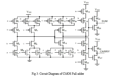
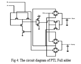
This paper presents the NMOS transistors (M1 TO M6) are used to implement the SUM output, and the PMOS transistors (M7 TO M13) are used to implement Cout output. CMOS FAs are very efficient and can perform addition of three one-bit binary numbers very quickly. They are used in a variety of applications, including high-speed computers, microprocessors, and digital signal processors. By employing a streamlined architecture that relies on a minimal number of transistors, this CMOS full adder design significantly reduces power consumption compared to conventional approaches. The use of 180nm technology further enhances energy efficiency by enabling precise control over transistor characteristics and minimizing leakage currents. This results in a substantial reduction in power dissipation, making the design well-suited for battery-powered applications and energy-constrained environments. Moreover, the compact nature of the design, achieved through the integration of transmission gates and pass-transistor logic, contributes to a reduction in propagation delay. This ensures faster operation and improved responsiveness, enhancing the overall efficiency and performance of the integrated circuit. The optimized transistor-level connections and carefully crafted signal paths further mitigate delays, allowing for seamless integration into high-speed systems requiring rapid data processing. Moreover the PTL Full adder with 10 transistors better than the CMOS Full adder in area efficient, performance. The PTL full adder design utilizes pass-transistor logic to perform addition operations. It typically consists of transmission gates and complementary pass-transistor pairs. These pairs are arranged to form logic gates, allowing signals to propagate through the circuit.
This paper presents a detailed investigation into the working principles and advantages of Pass-Transistor Logic (PTL) full adders. The PTL full adder design offers a novel approach to addition operations, leveraging pass-transistor logic to achieve efficient signal processing. The paper elucidates the operational mechanisms of PTL full adders and highlights their advantages in terms of reduced power consumption, low propagation delay, and compact design. Through comprehensive analysis and simulation results, the efficacy of PTL full adders in various applications is demonstrated, underscoring their potential for integration into modern integrated circuits.
Traditional full adder designs based on CMOS technology often suffer from limitations such as high power consumption and propagation delay. The introduction of PTL full adders addresses these challenges by adopting a novel logic paradigm that relies on pass-transistor networks. This section provides an overview of the motivation behind PTL full adders, outlining the need for efficient and low-power addition circuits in modern integrated systems. The working principle of PTL full adders revolves around the use of pass-transistor pairs to manipulate input signals and compute addition operations. This section delves into the operational mechanisms of PTL full adders, elucidating how pass-transistor logic facilitates signal propagation and processing. The intricate details of signal routing, complement generation, and output computation are discussed to provide a comprehensive understanding of the PTL full adder architecture.

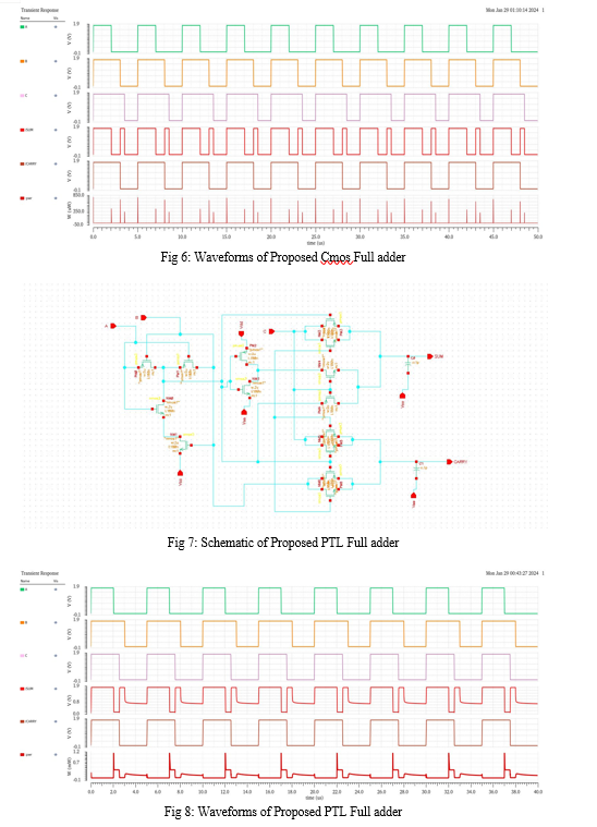
PTL full adders offer several advantages over traditional CMOS designs, including reduced power consumption, low propagation delay, and compact footprint. This section highlights the benefits of PTL full adders in terms of energy efficiency, speed, and integration density. Through theoretical analysis and experimental validation, the superior performance of PTL full adders is demonstrated, positioning them as a promising solution for next-generation integrated circuits. Experimental results from simulation and characterization studies corroborate the efficacy of PTL full adders in practical scenarios. This section presents comprehensive data on power consumption, delay, and area utilization, showcasing the superior performance of PTL full adders compared to conventional designs. Real-world applications and use cases are also discussed to illustrate the versatility and applicability of PTL full adders across different domains. By leveraging pass-transistor networks and Cmos networks, PTL full adders offer efficient and low-power solutions for addition operations in integrated circuits better than the Cmos full adders. The Pass-Transistor Logic (PTL) full adder emerges as the preferred choice over CMOS full adders due to its superior performance in terms of both delay and power consumption. By leveraging efficient signal propagation and minimizing resource utilization, PTL full adders offer a compelling solution for a wide range of applications, including high-speed data processing, low-power devices, and integrated systems.


Conclusion
In conclusion the design and implementation of full adders using both conventional CMOS and Pass-Transistor Logic (PTL) approaches. It aims to enhance the performance of electronic circuits, particularly in terms of power dissipation, delay, and area utilization. Through simulation and analysis using Cadence Virtuoso Tool in 180nm CMOS technology. The Pass-Transistor Logic (PTL) full adder emerges as the preferred choice over CMOS full adders due to its superior performance in terms of both delay and power consumption. By leveraging efficient signal propagation and minimizing resource utilization, PTL full adders offer a compelling solution for a wide range of applications, including high-speed data processing, low-power devices, and integrated systems.
References
[1] Mariano Aguirre-Hernandez, Monico Linares-Aranda, “CMOS Full-Adders for Energy Efficient Arithmetic Applications”, IEEE Transactions on Very Large Scale Integration (VLSI) Systems, 2011 [2] Hamed Naseri;Somayeh Timarchi, “Low-Power and Fast Full Adder by Exploring New XOR and XNOR Gates”, IEEE Transactions on Very Large Scale Integration (VLSI) Systems, 2018 [3] T.K. Schneider, A.J. Schwab;J.H. Aylor, “A full custom VLSI design methodology using Mentor Graphics design software in an educational environs”, Sixth Annual IEEE International ASIC Conference and Exhibit [4] Mehedi Hasan, Md. Jobayer Hossein, Mainul Hossain;Hasan U. Zaman, Sharnali Islam, “Design of a Scalable Low-Power 1-Bit Hybrid Full Adder for Fast Computation”, IEEE Transactions on Circuits and Systems II: Express Briefs, 2020 [5] Jyoti Kandpal;Abhishek Tomar, Mayur Agarwal;K. K. Sharma, “High-Speed HybridLogic Full Adder Using High-Performance 10-T XOR–XNOR Cell”, IEEE Transactions on Very Large Scale Integration (VLSI) Systems, 2020 [6] C. Senthilpari; Ajay Kumar Singh; K. Diwakar, “Low power and high speed 8x8 bit multiplier using non-clocked pass transistor logic”, IEEE Transactions on Very Large Scale Integration (VLSI) Systems, 2007 [7] Nan Zhuang; Haomin Wu, “A new design of the CMOS full adder”, IEEE Transactions on Very Large Scale Integration (VLSI) Systems, 1992 [8] Ningyuan Yin, Wanyuan Pan, Yihe Yu, Chengcheng Tang, Zhiyi Yu, “Low-Power Pass-Transistor Logic-Based Full Adder and 8-Bit Multiplier”, [9] Dempster, A.; Macleod, M. IIR digital filter design using minimum adder multiplier blocks. IEEE Trans. Circuits Syst. II Analog. Digit. Signal Process. 1998, 45, 761–763. [10] Prasad, D.D. Design and Implementation of Full Adder using Different XOR Gates. Int. J. Innov. Technol. Explor. Eng. 2020, 9, 1422–1426. [11] Amitha, M.; Deepa. Comparison between CMOS full adder and PTL full adder. IOP Conf. Ser. Mater. Sci. Eng. 2021, 1065, 012047. [12] Nan Zhuang; Haomin Wu, “A new design of the CMOS full adder”, IEEE Journal of Solid-State Circuits ( Volume: 27, Issue: 5, May 1992) [13] Nakul C. Kubsad, “Simulation and Analysis of different CMOS Full Adders for Delay Optimisation”, published on 2021.
Copyright
Copyright © 2024 J Rajitha, G Mahesh Babu, K Kavya, K Navina, T Tharun Teja, G Sujatha. This is an open access article distributed under the Creative Commons Attribution License, which permits unrestricted use, distribution, and reproduction in any medium, provided the original work is properly cited.

Download Paper
Paper Id : IJRASET58495
Publish Date : 2024-02-19
ISSN : 2321-9653
Publisher Name : IJRASET
DOI Link : Click Here
 Submit Paper Online

