Ijraset Journal For Research in Applied Science and Engineering Technology
- Home / Ijraset
- On This Page
- Abstract
- Introduction
- Conclusion
- References
- Copyright
Design and Implementation of 6-T SRAM using FINFET
Authors: Dr. P. Ravikiran, M. Manikiran, N. Bhavana Sai, J. Rathnakar
DOI Link: https://doi.org/10.22214/ijraset.2024.62994
Certificate: View Certificate
Abstract
SRAM is designed using conventional CMOS tech- nology to store data in memory. A lot of devices, including logic and memory, are having different issues as a result of the channel being lost of control. These include low leakage current, high power consumption, and short channel effects, which raise production costs and lead to significant changes in characteristics and decreased dependability. It is advised to employ FINFET based SRAM cells rather than traditional CMOS ones as a result of these problems. One of the primary elements that must be decreased in order to increase the stability of SRAM cells is thought to be power dissipation and leakage currents. The amount of power dissipation and leakage currents can be de- creased using a variety of low power methods. These include the Self Controllable Voltage Level (SVL) technique, Power Gating, Stacking technique, Variable Threshold CMOS (VTCMOS), and Multi Threshold CMOS (MTCMOS). Here, we suggest designing a FINFET SRAM cell using the 28nm technological approach and comparing its dynamic power consumption and stability to that of the 8T FINFET SRAM cell. Every simulation is carried out using the Cadence Virtuoso Tool.
Introduction
I. INTRODUCTION
The demand for a better storage system has led to the devel- opment of FINFET SRAM, a ground-breaking technology that offers a 7nm transistor design in response to advancements in the VLSI area. An increasingly common form of transistor design in semiconductor production is the FinFET (Fin Field- Effect Transistor), especially for advanced integrated circuits. Digital electronics frequently use volatile memory of the SRAM (Static Random-Access Memory) variety. Combining
FinFET technology with SRAM design can offer several advantages in terms of performance, power efficiency, and overall chip density. Here are some key aspects of FinFET- based SRAM, FinFET transistors have a three-dimensional fin-like structure, which enables improved regulation of the electron flow. This design helps in reducing leakage current and improving overall energy efficiency compared to tradi- tional planar transistors. Reduced Leakage Current: FinFETs are known for their superior control over leakage current, which is crucial for power efficiency in memory devices like SRAM. Improved Performance: The three-dimensional structure of FinFETs enables better gate control, leading to improved switching speed and reduced delay times. This can result in enhanced SRAM read and write performance. Higher Integration Density: FinFET technology allows for higher transistor density on a chip, leading to increased memory capacity within a given chip area.
Complex Fabrication: Compared to conventional planar transistors, the manufacturing process for FinFET-based SRAM is more intricate. The cost of production may go up as a result of this complexity. Design Difficulties: Al- though FinFETs provide better performance, there are new design issues to take into account when creating circuits with them, like higher parasitic capacitance and unpredictability. Commonly found in cutting-edge semiconductor devices, such as high-performance Research and development efforts are still being directed towards enhancing FinFET technology and resolving issues related to its use in graphics processing units (GPUs), SRAM and other integrated circuit processors, and other memory-intensive applications. Alternative transistor designs, including nanosheet transistors, are constantly being investigated in order to get around some of the drawbacks and difficulties that come with FinFET technology.
Power consumption has become an important design con- sideration for VLSI systems and microprocessors, especially for SRAM architecture.Three different causes have led to the following result: 1) Most modern VLSI designs include a large cache built from SRAM cells as part of the System-on- Chip (SOC); 2) as deep sub-micron technology advances, the die’s total area becomes smaller and smaller; this smaller area causes a temperature problem in VLSI circuits, so reducing power consumption is necessary to lower the chip’s tempera- ture; and 3) as portable devices become more and more pop- ular, lower power VLSI circuits become more commercially viable in the consumer electronics industry.
These considerations have prompted several scientists and SRAM designers to investigate methods for lowering power dissipation.
One of the current forms of SRAM cells, the carbon nanotube field effect transistor (CNFET), has the po- tential to replace the standard MOSFET because to its energy economy and fluctuation tolerance. Future nano-electronic devices may be replaced by a carbon nanotube field-effect transistor (CNFET). Chemical stability, high-speed operation, and high-K compatibility are only a few of its exceptional electrical characteristics. In order to reduce both static and dynamic power, we present a unique 8-T SRAM cell in this work that is based on a carbon nanotube field effect transistor (CNFET).
Storage cells are essential for the power, speed, and perfor- mance of the microprocessors and microcontrollers in digital circuits such as System-on-Chips (SoCs). These memory ar- rays take up a large portion of the chip surface. Because of this, the majority of the chip’s power actually comes from these memory cells. Various SRAM cell layouts have been published in academic articles, with the major focus being on reducing cell area, device count, and leakage power. SRAM cell sizing is further complicated by the higher transistor leakage observed in the CMOS nodes with inferior technology. Memory architectures that use power supply shaped like trapezoidal pulses have been discovered to lower the SRAM cell’s power consumption.
II. LITERATURE REVIEW
The main issue with standby leakage in electronics devices is going to have a big effect on the electronics industry over the next few decades. Additionally, as CPU data processing frequency increases, so does the requirement for cache mem- ory. The layout of the cache memory is likewise done with SRAM. Numerous low-energy methods are being explored to reduce current leakage. The primary programme utilised in the creation of digital circuits is Full MOSFET 6T SRAM mobile. The inherent density of the chip rises as technologies continue to be downscaled. A crucial concern is the stability and dependability of any memory device, including DRAM and SRAM, under various settings.
Presenting a 6T SRAM Cell Analysis in Various Technolo- gies to analyse the Static Noise margin of the cell. Together with the read channel’s isolation from the real internal storage nodes, this takes out the read-disturbance.Additionally, it uses a write-assist mechanism to carry out its write operation in pseudo differential form using a write bit line and control signal[1]. In this study, a 6T SRAM cell for 90nm and 180nm technologies has been created. The Cadence Virtuoso tool has been applied to modelling and design. Using nmos1V and nmos2V cells in 180nm and 90nm technologies, the static noise margin for SRAM has been determined. SNM decreases with shrinking technology, as expected, and CMOS 1v transistors have been found to have better SNM than CMOS 2v transistors[1].
The publication FINFET-based 6T SRAM Design and Im- plementation for Low Power Applications was proposed to develop a FINTET SRAM cell using the MTCMOS tech- nology and compare its dynamic power dissipation with that of a FINTET SRAM cell. Using 32nm technology, Synopsis Hspice Tool is used for all simulations[2].Transistors with varying threshold voltages (Vth) are used in a type of CMOS device known as multi-threshod CMOS (MTCMOS) to either increase power or minimise latency. Effectively, the transistor’s threshold voltage is the gate voltage at which an inversion layer forms at the interface between the substrate (body) and gate oxide layer. Low Vth devices are helpful for minimising clock durations on important delay lines because they flip quickly. One drawback of low Vth devices is that their static leakage power is significantly higher.[2]
The 32nm technology is utilised to model MTCMOS Fin- FET SRAM using the Synopsis HSpice tool. The dynamic power dissipation, which is essentially the product of the power supply and the current, is calculated. In the MTC- MOS FINFET SRAM case, the dynamic power dissipation is 21.88nw, or about equivalent to 22nw. The MTCMOS tech- nique reduces dynamic power dissipation more than FINFET SRAM does[2]
The work Memristor-Based SRAM Cell and Low Power 6T SRAM Cell with 45NM CMOS Technology: Stability and Performance Analysis is designed in the Cadence tool to contrast the memristor SRAM with SRAM’s performance.This memristor is long-lasting. This method reduces leakage current by lowering the stored data limit without a power source by boosting packing density and allowing on-chip (SOC) devices. The methods we build to use the field have a maximum execution speed based on SRAM[3].
This investigation aims to aid in the characterization of the battery-bit column Drain. Examining the margin’s quantity is the primary goal of this test. in the course of reading a lengthy column. This analogy, which represents the most design possible, ought to act as a compass within the matrix of physical memory. A bit cell can be used to analyse the leakage current[3].
III. PROPOSED METHODOLOGY
This section outlines the suggested methodology for Design and Implementation of 6-T SRAM using FinFET. The specific actions involved in writing and reading in FinFET 28nm technology is employed in the proposed SRAM cell.
When the node is discharging from a charged state or is in a recovery phase, the adiabatic circuit regenerates energy. The adiabatic approach contributes to a reduction in the circuit’s overall power loss and energy loss in this way. In high-density systems, incorporating this logic into memory cell architecture can result in significant power savings. The following literature contains descriptions of several adiabatic technique schematics that are controlled by trapezoidal power rails.
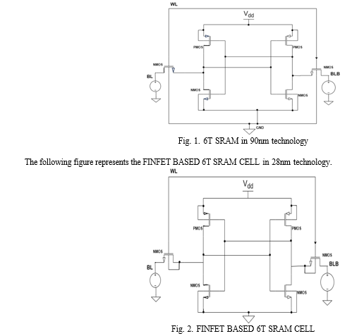
To store a single digital bit of logic 1 and logic 0 data, a six- transistor SRAM cell normally consists of four transistors that combine to generate two inverters. The storage cell’s storing and retrieving functions are controlled by two access main transistors. A main six-transistor SRAM cell with a dual bit line is composed of two CMOS inverters, which are stabilised in their respective states by feeding back the output voltage of one inverter into the input of the other.
To read from or write to the memory cell, bitlinbar, wordline, and bitline are the primary input transistors. The WL is primarily lower in standby mode, which disables the access transistors. Right now, the NOT-gates are in the reverse configuration. Furthermore, when the p-channel MOSFET in the left inverter is on and the p-channel MOSFET in the inverter two is off, there is a high voltage at Qbar and a low Q. Data is mostly stored in the BL, and reverse data is stored in the bitlinebar, also referred to as the inverse bit line. Flipping the wordline to high turns on the access transistors.
The bitline driver, which is far more powerful, has the ability to override the inverter transistors. To avoid data loss, the access FinFET can mostly be turned off after the data has been stored in the inverters. The word line is activated to turn on the access devices when the bit lines detect the data.

IV. READ OPERATION
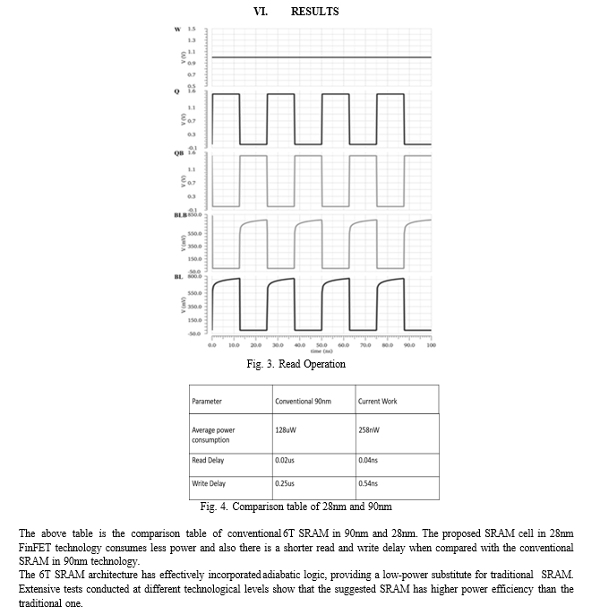
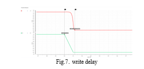
A certain procedure in SRAM requires the WL to be high at all times. Read operations will be executed using memory. For memory, let’s say Q is 1 and Qb is 0. To perform read operations, the WL is increased. The two output lines are BL and BLB, and since node potential Vdd is already present at bitline and bitlinebar, the BLs are already pre-charged. Since bit Q is at the top of the circuit, there is no possible drop. There must be a potential difference between Qb and the node potential since Qb is 0 at BLB. Because of the discharge, there is a current flow in the circuit as a result of the potential at bit b falling. bitline and bitlinebaer serves as an estimator since it is connected to the sensing amplifier. The output of the sensing amplifier is one when BLB is smaller. Assume that in memory, Q is 0 and Qb is 1. The potential difference causes an electrical discharge to occur at bit and Q in the diagram. The gadget ought to have certain ratios so that Q is within the P2 designated zone.
We call this the read limitation. The output is zero as the bit potential decreases. The result is 0 when Q = 0. Therefore, in both cases, the read operation was successfully confirmed.
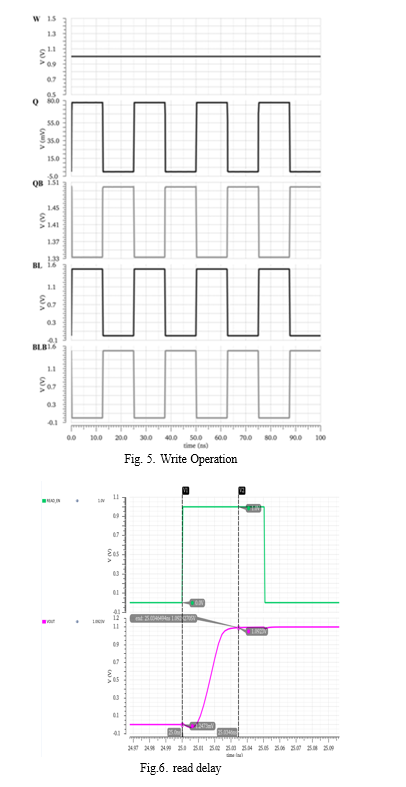
V. WRITE OPERATION
Here Vdd is charged to write a ’0,’ BL is discharged through the ground. Following these two procedures, WL is set HIGH and the data is written into the cell. Consider memory bits with Q is 0 and Q is 1 value. There are two input lines in the write operation, BL and BLB . To regulate the input lines, first link bitlinebar to the ground, resulting in a large potential difference between Qb and bitlinebar.We can change the precise ratio of the devices to make pass transistors stronger than pmos in order to set Q to 1, which is necessary in order to write one to the SRAM cell. Q will therefore be one. Initially, Q is 1 after the particular action, signifying that the write operation into memory was successful.
SENSE AMPLIFIER
In order to provide accurate monitoring, the sense amplifier finds the BL and BLB. While consuming less power to operate, it increases the speed at which memories are read. Enhancing the potential difference on the BL and BLB during write and read operations is the main function of the sensing amplifier. Transistors NM2 and NM0 are turned on while NM1 is turned off, activating PM1 and PM0, to read ”1,” which is composed of BL is 1,BLB is 0. VDD rises as a result at the output logic. Transistors NM1 and NM2 turn on when the logic ”0” is read using BL=0 and BLB=1, deactivating PM1 and PM0. Meanwhile, NM0 turns off.Consequently, the output shows logic ”0” and the VDD and output are not connected. The wave shape below shows that when se (Sense enable) is strong for a specific amount of time, the data contained in the BL is read out. The 6T SRAM cell used in this architecture has an adiabatic charging of the BL in write mode. Both the suggested SRAM cell and the traditional 6T-SRAM are made up of two switching transistors, MP1 and MN1 (pmos, nmos), as shown in Fig.1 Multiple transistors along the rows can share the switching transistors when there is an MCPL(MOS-controlled Power Line) node.
In write and read operations, the primary purpose of the sensing amplifier is to increase the potential difference on the BL and BLB.
A. Power Consumption
Leakage currents passing through transistors in the memory array and related control circuitry are the main source of static power in SRAM. The CMOS transistors used to implement the memory cells have gate leakage and subthreshold leakage processes, which cause these leakage currents.
When there is a tiny voltage over the source and drain terminals of a transistor, a faint current flows through the tran- sistor, leading to subthreshold leakage. When the temperature rises and the threshold voltage decreases, the leakage current grows exponentially. The non-ideal behaviour of the gate oxide layer, on the other hand, causes gate leakage, which permits a tiny current to pass through the gate terminal even when it shouldn’t be conducting. The arrangement of the memory cells, supply voltage, temperature, process technology, tran- sistor properties, and other parameters must all be taken into account when calculating the static power consumption of SRAM. To calculate the total static power dissipation, the leakage currents of each transistor in the SRAM array are commonly estimated and added together.
The following is the formula to determine static power consumption:
Static Power = Leakage Current * Supply Voltage
To calculate the overall static power dissipation, multiply the leakage currents of all the transistors in the SRAM array by the supply voltage.
During read and write operations, internal node capacitances are charged and discharged, which is the main cause of dynamic power consumption in SRAM. The simple formula that follows can be used to compute it:
Dynamic Power = Activity Factor * Capacitive Load * Voltage2 Frequency
You can average the static and dynamic power throughout the appropriate time period to determine the average power consumption over time. This can be stated as follows:
Average Power = (Static Power + Dynamic Power) / Time where ’Time’ stands for the length of time that you are calculating the average power usage.


Conclusion
The implementation of a 6T Static RAM memory cell at 28nm advanced FinFET technology is described in this paper. The implementation was accomplished by choosing consistent results at various states of memory write operation and memory retrieve operations.A precise estimation of a standard 6T cell is also included in this method, which is based on a variety of well-implemented FinFET devices in the sub-28nm region and is also compared with 90nm. Beyond 32 nm technological nodes, FinFET is a possible replacement for MOSFET that will eliminate the difficulty and barrier that conventional MOSFET faces. SRAM can now be further scaled due to the FinFET’s larger subthreshold slope, decreased random dopant fluctuation, and relief of high-K material for the gate oxide. However, when technology nodes drop, parasitic RC becomes a concern in SRAM design due to SRAM coupling capacitance and wire scaling. RC delay is an undesirable yet unavoidable problem.
References
[1] Prithu Jain, Shalabh Bansal, Vandana KhannaDepartment of EECE, The NorthCap University presented a 6T SRAM Cell Analysis in Various Technologies to analyse the Static Noise margin of the cell. [2] Madhuri Yenuganti,Thaherunnisa Syed,Tarun Kumar Undavalli devel- oped An MTCMOS-based FINTET SRAM cell utilising the article FINFET-based 6T SRAM Design and Implementation for Low Power Applications. [3] S V S V Prabhu Deva Kumar, Shaiwal Suman, Arup Sarkar, Vivekanand Kushwaha proposed a work Memristor-Based SRAM Cell with 45NM CMOS Technology Low Power 6T SRAM Cell: The Cadence tool’s stability and performance analysis feature is intended to Compare the performance of SRAM with that of the memristor SRAM. [4] Cell Stability Analysis of Conventional 6T Dynamic and 8T SRAM Cell in 45nm Technology, S. K. Dhanumjaya, M. Sudha, Dr. M.N. Giri Prasad, and Dr. K. Padmaraju, International Journal of VLSI design and Communication Systems (VLSICS), Vol.3, No.2, April 2012. [5] Source/Drain-Doping Engineering for Optimal Nanoscale FinFET De- sign, V. P. Trivedi and J.G. Fossum, International SOI Conference, pp. 192-194, 2004. [6] Leakage current reduction in FinFET based 6t SRAM cell for minimis- ing power dissipation in nanoscale memory is presented by Saurabh Khandelwal and Vishal Gupta at the Nirma University International Conference on Engineering (NUiCONE), 978-1-4799-9991-0/15/ 2015 IEEE. [7] The paper ”New SRAM Cell Design for Low Power and High Reliability using 32nm Independent Gate FinFET Technology” was presented at the IEEE International Workshop on Design and Test of Nano Devices, Circuits and Systems (978-0-7695-3379-7/08) in 2008 by Young Bok Kim, Yong-Bin Kim, and Fabrizio Lombardi. [8] Design of a 32 nm independent gate FinFET based SRAM cell with enhanced noise margin for low power application, M. Rahman and R. Mahapatra, 2014 International Conference on Electronics and Commu- nication Systems (ICECS), 2014 [9] ”Design and Verification of Low Power SRAM using 8T SRAM Cell Approach,” by Nahid Rahman and B. P. Singh, was published in April 2013 in the International Journal of Computer Applications (0975–8887), Volume 67–No. 18. [10] ”Low Power Single Bit line 6T SRAM Cell With High Read Stability,” Budh Aditya Majumdar and Sumana Basu, IEEE 2011 International Conference on Recent Trends in Information Systems.
Copyright
Copyright © 2024 Dr. P. Ravikiran, M. Manikiran, N. Bhavana Sai, J. Rathnakar. This is an open access article distributed under the Creative Commons Attribution License, which permits unrestricted use, distribution, and reproduction in any medium, provided the original work is properly cited.

Download Paper
Paper Id : IJRASET62994
Publish Date : 2024-05-30
ISSN : 2321-9653
Publisher Name : IJRASET
DOI Link : Click Here
 Submit Paper Online

