Ijraset Journal For Research in Applied Science and Engineering Technology
- Home / Ijraset
- On This Page
- Abstract
- Introduction
- Conclusion
- References
- Copyright
Design and Implementation of Braun Multiplier using Verilog: Research
Authors: Anukrati Sharma, Aparna Mittal, Anshika Singh
DOI Link: https://doi.org/10.22214/ijraset.2024.62374
Certificate: View Certificate
Abstract
Multiplication is widely used in places like digital signal processing, image processing, instrumentation that require multilayer components. Carry Save Adder and ripple carry adder both are used in parallel processing architecture. They are widely used for signed multiplication i.e. for both negative and positive numbers. We have now designed a Braun multiplier (BM) to improve the speed, power and area capability. We are using the Xilinx tool to verify Braun multipliers using Verilog. We are taking the following considerations: checking using FPGA based instruments and implementing code using Verilog-VHDL. The adders are integrated into multipliers. The result of this research is to modify BM to improve the performance along with reduction in power consumed and also using less area.
Introduction
I. INTRODUCTION
An elementary arithmetic operation is multiplication. They are used in many DSP applications, including filtering and FFT, and they frequently cause large delays in processing times and occupy a sizable portion of silicon in DSP systems.
Multipliers are essential components in digital signal processing and FPGA-based applications, perhaps because they consume more power and space than other devices. Multipliers, which in turn depend on adders, are essential components of DSP and FPGA-based systems because they provide power, speed, and area. Therefore, the latency can be reduced by using adders.
The need for efficient operations that involve multiplication is growing due to the increasingly complex nature of today's computer tasks. With its creative design, the Braun Multiplier offers a workable answer by reducing the number of required processes. This makes it a viable option for applications requiring accurate and speedy multiplication, such as digital signal processing and encryption. Verilog offers a variety of abstraction levels at which the behaviour of the Braun Multiplier can be explained, from the high-level algorithmic view to the low-level digital implementation. We can simulate the Verilog model to confirm its validity, optimise its efficiency, and validate its usefulness.
This work is organised to provide a succinct overview of some of the innovative methods and techniques that different authors have used to discuss Braun multipliers that use FPGA.
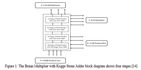
Figure 1 illustrates how a Kogge stone adder and Braun multiplier were employed in one of the publications that we examined to increase the area yet decrease the delay. Kogge Stone Adder and Ripple Carry Adder findings were additionally compared in this study.
A different study offered an innovative form for creating and evaluating a Braun array multiplier; they used multiplier modelling and simultaneous prefix adders to boost the multiplier's functionality. The multiplier multiplies binary numbers more quickly by utilising the 4-bit precession and ripple carry adder. The results show that the new techniques can be used to construct and analyse the multipliers.
A Field-programmable Gate Array (FPGA) is a kind of integrated circuit designed exclusively to be incorporated into another one. The FPGA's layout is designed to facilitate a wide range of operations. The hardware Braun's Multiplier implementation in the Virtex-4, Spartan-3E, and Verilog HDL has been investigated in this article. The multipliers were developed in Verilog HDL, synthesised, and simulated using ISE 11.4 Design Architect after being executed in ISE 12.4 design tool.
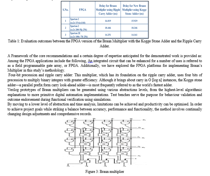
Along with simulation and multiplier synthesis, the Braun Multiplier can also be implemented in FPGAs deploying various FPGA platforms, such as Spartan-3E, Virtex-4. The Braun multipliers can be executed on Field Programmable Gate working with a range of technologies and resources, as we will describe further. FPGAs are extremely versatile and adaptable integrated circuits, which are chips that can be tuned and set up for a variety of purposes, methods and techniques as shown in Table 1.
Xilinx (version 14.7) ISE design tools along with Verilog (version 14.7) HDL are the primary application programs used in implementing the Braun multipliers onto FPGAs.
II. LITERATURE REVIEW
In the paper named "Implementation of parallel multiplier based on Booth computing method using FPGA"[1] proposed by B. Jeevan, P. Samskruthi, P. Sahithi and K. Sivani in the year 2022, put forward a method using booth encoding which was developed for partial products. This process is divided into two parts. The final product is considered as the third part. This paper provides various architectures of multiplication. It also gives us information that the parallel multiplier is faster as compared to serial multiplier. In this paper they have discussed the serial of action.
In the first step we get partial products, in the second step we add the two rows and get the result in two rows, in the last step we obtain the final result. This multiplication is performed using the booth encoding method in this paper. To get the partial product booth encoding scheme is proposed for obtaining the operational stability from the existing plans. During multiplication the partial product addition is obtained with martial product reduction tree or OPPT method.
In the year 2020 a paper entitled “Design of High-Speed Multiplier using Parallel Prefix Adder” [2], presented by N Venkateswara Rao, B Navya Surya Ratnam, et al. this paper presented the idea that different types of Kogge stone adder developed using various logic gates can be used like 22T XOR,14T XOR and 12T XOR. This paper compares the new model of Braun multiplier with the old method with reference to delay.
Taking the new method the 22T-XOR Kogge stone adder has 222 transistors and gives a delay of 101.01ps. The 14T-XOR Kogge stone adder has 174 transistors and obtains a delay of 152.91ps. And the last 12-XOR Kogge stone adder has 162 transistors and gives a delay of 21.03ns. The new method of Braun multiplier has inputs equal to 4X4 and outputs equal to 8. We have more output pins because a large delay is produced at the output side. The output pins are replaced with Kogge stone adder to reduce the delay.
In a research paper “Design of Efficient Braun Multiplier for Arithmetic Applications” [3] proposed by Telagamalla Gopi in the year 2020, this paper suggested the concept of using pyramid adders. In applications like DSP and FPGA- based applications, multipliers are used as they require more power and area as compared to other devices. Area, power, and speed are considered as the most important features in applications like FPGA and DSP. All the above parameters depend on multiplication which then depends on adders.
Using pyramidal adders which have both the half adder and full adder increase the performance and reduce the quantity of gates required in the multiplier and also decrease the latency. The modern pyramidal adder that contains XNORs and MUX instead of full adder and half adders uses less gates and less delay is used. As MUX selects only one output among many inputs. Using XNOR and MUX in pyramidal adder reduces the delay.
A paper titled “Comparative study of Braun’s Multiplier Using FPGA Device ''[4] was given by Anitha R, Bhagya Veereswaran V in 2019. In this paper a bypassing method is proposed to decrease the computation delay and enhance the use of resources. For designing the Braun multiplier, it is comparing column bypassing and row bypassing technique along with full adder is replaced with fast adder. In this paper it is implemented on Virtex 6, Virtex 5 and Spartan 3E.
In this paper they have also used fast adder to decrease slices. The value of delay and look up table is also decreased in comparison to the ol method. It is found that Virtex-6 uses a less powerful FPGA chip which has reduced combinational path latency and also decreased the average pin delay. Hence comparing an FPGA device with virtex-6, virtex-6 gives better results with low power. Braun multiplier is mainly used in applications like image processing, multimedia technology and digital signal processing.
A research conducted on ‘An Efficient Multiplication of Braun and BW Multiplier’ [6] authored by K.Sireesha, Dr.T. Lalithumar, T.V.Nirmala, and S.Haneef during 2018. This paper tells us about the usage of multipliers in the field of signal processing and digital signal processing. This paper also tells the importance of using Braun multipliers that can be used for multiplying positive and negative numbers in parallel architecture.
The paper also looked into the design of adders based on CMOS, split path data driven dynamic logic and domino dynamic logic. The important conclusion that we can obtain from this paper is that it reduces the power consumption as well as the delay, which in turn improves the speed and also decreases area in the circuit. The changes made in Braun multiplier and BW improved the performance of the multiplier in comparison to the old design and hence making BM a important component in DSP applications.
A paper titled “Novel Approach to Design Braun Array Multiplier Using Parallel Prefix Adders for Parallel Processing Architectures” [7] by Kunjan D. Sharma, K.D. Amit Kumar, D.S. Rashmi, H.R. Shilpa, and C.R. Vidashree in 2018. This paper focused on the approach of design of Braun array multiprocessor (BAM) along with Parallel prefix Adders (PPA). It's all so known for its fast carry generation network and are the highest speed adders available.
The study of brent kung, Kogge stone and other common types of PPA adder is being conducted to find the worst possible scenario in terms of delay, power consumption and number of transistors being used along with little emphasis on low power being consumed.
This method shows the importance of adders and microprocessors to meet the speedy processing necessity of current signal processing systems.
A research paper titled “A Review on Various Multipliers Designs in VLSI ''[9] proposed in the year 2015 by Khuraijam Nelson Singh and H. Tarun kumar introduced a novel design. A dual array tree structure and the temporal tilling method are used in the design. We also study several approaches to the optimization of Wallace array multipliers. We have built a low power array multiplier with a modified booth encoding method, based on the Nikhilam sutra. The performance of the new multiplier is 30% and 50% better than that of the conventional CMOS.
In spite of being the most power-hungry and delayed part of the research, Shivaling S. Mahant's demonstration indicates that the array multiplier may be effectively optimised. Choi Junghwan and associates (2000) and Shetti and associates (1999). With Booth encoding, the Wallace tree multiplier is the fastest and most efficient optimization for improved display. Effective planning of a Wallace tree multiplier with Booth encoding can also be achieved as a pipelined structure, as shown by Rahul D. Kshirsagar and colleagues (2013) to rise.
Jyoti Sankar Sahoo and Nirmal Kumar Rout are the authors of the 2015 book "Comparative Study of Different Low Power Designs of Braun Multiplier using Double Gate MOSFET at 45nm Technology" [10]. This study focuses on the AND gate and double gate MOSFET designs used in the Braun multiplier. An essential component of the multiplier structure is the AND gate. The Cadence program is utilised in the implementation of the AND gate and power multiplier designs. The results are given for different designs of Braun multipliers.
This paper discusses the design of a low-power Braun's multiplier using three different low-power technologies and a double-gate MOSFET in a full addition. A power delay product is appended to the delay product. We make comparisons and computations between the three designs. Using a complete DOUBLE-TOUCH MOSFET adder and a DOUBLE-TOUCH MOSFET sleeping array of AND doors, the third design demonstrates how technology can be preserved while improving power savings. dissipation of power delay products, delay, and energy. In 45 nm and Cadence Virtuoso Tool technology, three low-power, high-speed Braun multifunction are utilised.
A Research paper titled "Braun's Multiplier Implementing FPGA Using Bypassed Techniques" was released in 2011 [15]. Using Kogge Stones adders in conjunction with the Braun Multiplier's capabilities, Anitha (R) and Veereswara (B) demonstrated a revolutionary multiplication method. Using a normal digital multiplication technique, the Braun Multiplier consists of a [N-1] Carry-Save Adder and a Ripple Carry Adder. The new Braun Multiplier that was suggested and the current one were compared in research.
To determine the advantages and disadvantages of the new Kogge Stone multiplication method, the research evaluated factors such as speed, area use, and performance. Kogge Stone and Adder This adder has a great reputation due to its fast carry bit computation. It is incorporated to improve performance even if it takes up more space. A few of the many applications for the adder are data preparation, result handling, and prior processing. It can generate carry signals with O(log n) temporal complexity and amazing efficiency. There is a noticeable decrease in the total latency of the adder.
The Research was titled "Braun's Multiplier Implementation using FPGA with Bypassing Techniques" In order to create Braun's Multiplier, Anitha R. Bagyaveeraswaran V., India, [15] conducted research using the "fast addition" method in combination with FPGA technology and cutting-edge bypassing techniques. This research was motivated by the prohibitively high cost of developing ASICs and the fact that multipliers are essential operations that support a wide range of applications, such as digital signal processing (DSP) and image processing.
Braun multipliers can be implemented in FPGAs at a lower cost using FPGAs. A comparison of FPGAs based on various platforms (Spartan-3E/Virtex-4/Virtex-5) and FPGA Low Power (Virtex-6) is included in the study. The following are the study's findings: The number of slices, delay, and LUTs used are much less than in typical architectures.
A research article titled "Design and analysis of low power Braun multiplier architecture" was published [16]. The primary objective of the research is to investigate the potential power dissipation caused by multipliers within Digital Signal Processing, or DSP, blocks. The main source of power dissipation in these kinds of applications is multipliers. The ways to achieve power optimization across different CPU modules are also examined in the current investigation.
The study offers a thorough examination of the various ways that DSP blocks, multipliers, and other elements contribute to power dissipation. It also examines the various power-optimization strategies for CPU components. The research concludes with a comparison of the power and design achievable utilising low-power sign array multipliers. Full and partial adders are the fundamental building blocks implemented in the paper and are thought to be crucial for multiplier creation. After including such low power adders into its suggested multiplier architecture, the paper evaluates the results.
III. EXPERIMENTAL DETAILS
A. Hardware and Software Requirements:
- FPGA development board (e.g., Xilinx Spartan-3E)
- Verilog coding tool (e.g., Xilinx ISE)
- ISIM Simulation and synthesis software
Typically, an FPGA application stores configuration images in a single, non-volatile, memory. Illustrating the new capabilities of the kit board, it has three different configuration memory sources, all of which need to work well together.
The additional configuration functionality makes the starter kit board a bit more complicated than typical applications in the Spartan-3E FPGA family. On-chip circuitry simplify the device programming experience in typical applications.
B. Braun Multiplier Implementation:
- Xilinx ISE software will be used to write and synthesis the Verilog code for the Braun multiplier.
- The design will be implemented on the FPGA development board.
- The Verilog code will be mapped to the FPGA device during implementation, and it will be programmed to carry out the multiplication operation.
C. Testing and Verification:
- The functionality of the Braun multiplier will be verified through simulation using the Verilog testbench.
- To ensure the accuracy of the result, test vectors will be fed into the multiplier.
- To make sure the multiplier is operating as intended, the simulation's output will be examined.
IV. THEORY
A. RTL schematic and Technology Schematic
The Register Transfer Language (RTL) describes the implementation logic of a memory chip circuit. RTL design is an abstraction level in digital circuit design. It describes the behaviour of the circuit in terms of the data flow between the registers, as well as the logic that processes that data as it flows between the registers.
RTL design refers to the process of describing a circuit’s behaviour by describing the data flow between registers, as well as the logic used to manipulate that data. Verilog, an HDL (Hardware Description Language), allows engineers to describe how data flows between registers, and how it’s processed by the combined logic between those registers.
This approach allows engineers to provide a detailed description of the operation of a circuit, while abstracting from the details of the physical implementation. By concentrating on the data flows and logic operations of a digital circuit, the RTL design process allows for efficient simulation and verification, as well as synthesis, of digital circuits.
RTL design is a fundamental abstraction in the field of digital circuit design, providing a bridge between the high-level concepts of design and the details of hardware implementation.
B. Technology Schematic
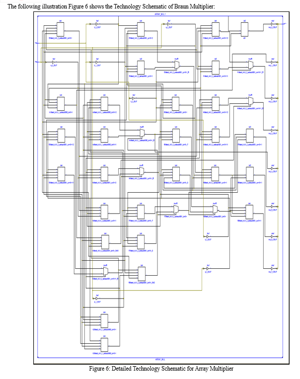
A technology schematic is a visual representation of how a digital system such as the Braun multiplier works. It describes the structure and connections of important parts such as AND gate and adders. It explains the binary multiplication process, making it easier to understand, design and analyse.
A technology schematic is essential for the engineers and designers who are responsible for implementing the multipliers in digital hardware. It allows them to plan and troubleshoot and optimize the performance of the system.
V. RESULT
A. RTL Schematic
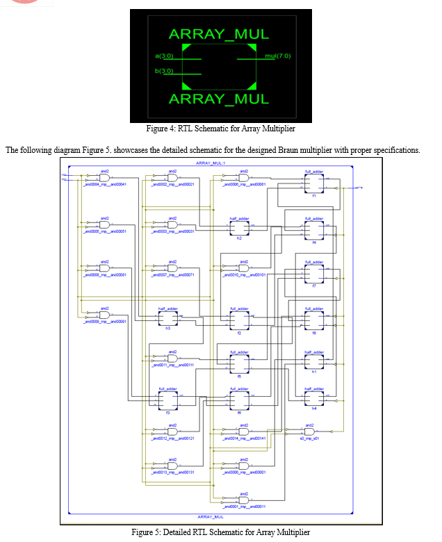
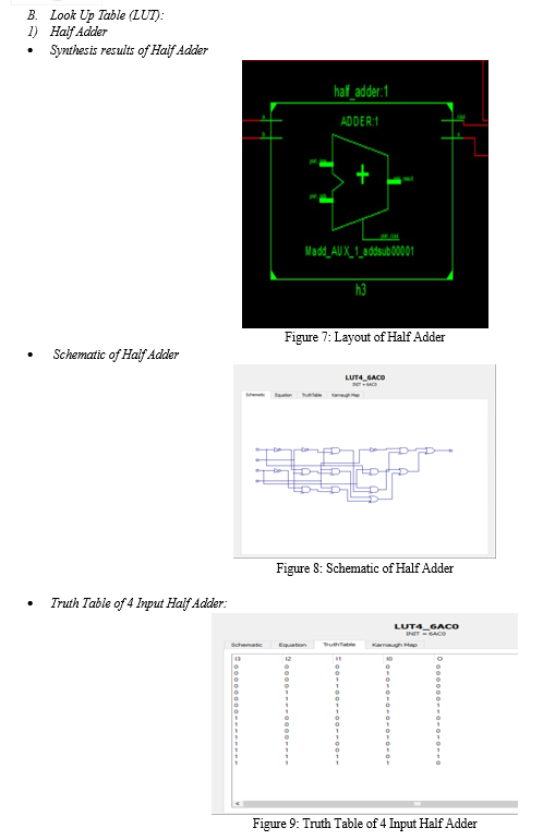
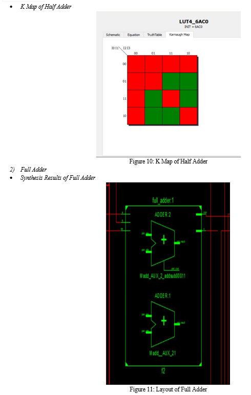
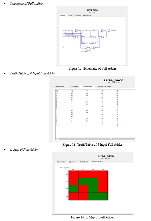
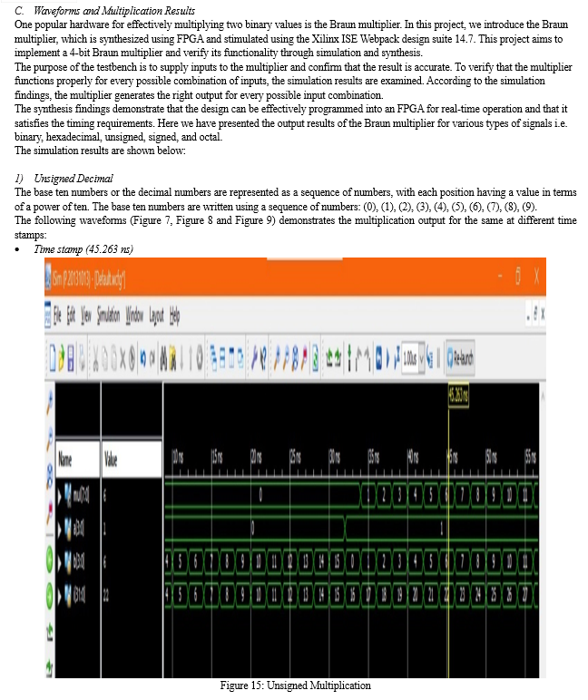
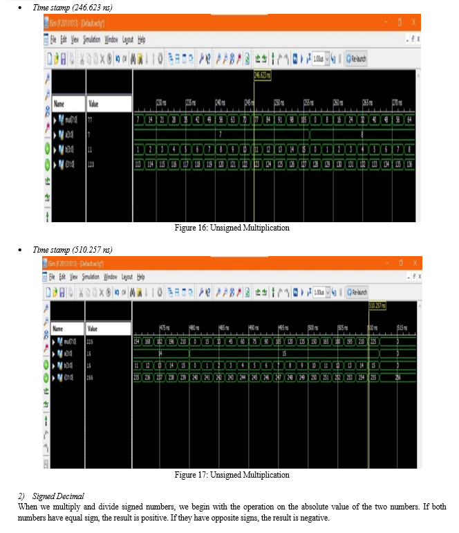
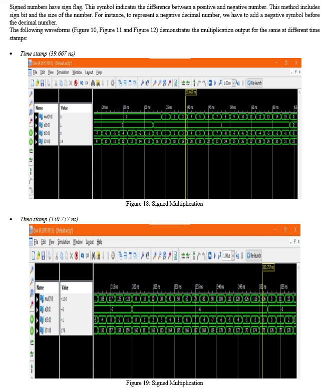
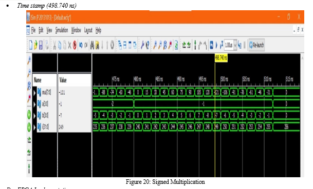
Figure 4 showcases the layout design of RTL Schematic for Braun Array Multiplier
D. FPGA Implementation
Field-programmable gate arrays (FPGAs) are a type of semiconductor device that consists of a number of programmable logical blocks and configurable interfaces. Unlike ASICs, which are designed for a particular purpose and fabricated as fixed-configuration devices, FPGAs can be programmed and reconfigured after manufacturing.
In the past, FPGAs were chosen for lower speed/ complexity/volume designs. Today, FPGAs can easily exceed 500 MHz performance. In addition to unprecedented logic density increases, FPGAs offer a wide range of other features such as embedded processor, DSP block, clocking, high-speed serial, and even lower price points. FPGAs are an attractive proposition for almost any design.
The FPGA (Field Programmable Gate Array) Implementation of Braun Array Multiplier is given in the following figure:
Conclusion
In this paper we have presented a Braun multiplier using carry save adder and ripple carry adder. We have implemented it using Verilog language and design using Xilinx ISE Webpack design suite 14.7. We have designed this multiplier so that it can reduce the delay and hence it can give the best results in terms of speed, area and power as compared to the conventional multipliers. We have designed this multiplier for signed multiplication so that we can get more precise results. The conventional multiplier is designed using full adders and AND gate which uses more delay and power. This type of multiplier is widely used in applications like Digital Signal Processing and image processing where the response of the system is much more important than the cost. Future Scope 1) Optimization: There is always room for improvement in terms of area, power, and performance. Researchers might look at low-power design techniques, pipelining, and parallelism to increase the efficiency of the Braun Multiplier. 2) Scalability: Currently, the Braun Multiplier is used to perform 4x4 or 8x8 bit multiplication. In the future, the focus should be on increasing the Braun Multiplier\'s ability to handle inputs with larger bit widths, such as 16x16 or 32x32 bits. 3) High-level synthesis: High-level synthesis (HLS) tools can be used to automatically construct Braun Multiplier designs from a high-level description (like C/C++ code). This could help save design time and increase output. 4) Verification: This is an important phase in the design of digital circuitry. Researchers may consider using advanced verification techniques such as hardware acceleration, limited random testing, and formal verification to ensure the accuracy of Brownian multiplier designs. 5) FPGA implementation: A field-programmable gate array (FPGA) can be used to house the Braun multiplier for hardware acceleration. In order to attain better performance, future research may focus on refining the architecture of FPGA implementations, exploring different architectural choices, and concentrating on certain FPGA families.
References
[1] “Design of Efficient Braun Multiplier for Arithmetic Applications”, International Journal of Science and Research (IJSR) ISSN by Gopi T: 2319-7064 SJIF (2020): 7.803. [2] “High-Performance VLSI Architecture for Braun Multiplier”, International Journal of Innovative Technology and Exploring Engineering (IJITEE) ISSN by Karunakaran S, Poonguzharselvi B, 2278-3075 (Online), Volume-8 Issue-10, August 2019. [3] “A Novel Approach to Design Braun Array Multiplier Using Parallel Prefix Adders for Parallel Processing Architectures” Second International Conference, by Shinde, Kunjan & Kaller, et al., ICSCS 2018, Kollam, India, April 19–20, 2018. [4] Design and performance analysis of multipliers using Kogge Stone Adder”, 3rd International Conference on Applied and Theoretical Computing and Communication Technology ,by Raju A,Sa S.K, 2017. [5] “Implementation of Baugh-Wooley Multiplier and Modified Baugh Wooley Multiplier Using Cadence (Encounter) RTL”. IJSETR. 4. 293-298, International Journal of Science Engineering and Technology Research (IJSETR), by Mahajan, Mukesh,Aswale, et al, vol. 4, issue 2, pp. 293 – 298, Feb. 2015 [6] Vinay B.Chetan C.S. , Biradar et al, “Performance Enhancement of 32-bit Carry Select Adder by Employing RTL Optimization Techniques”, International Research Journal of Engineering and Technology, IRJET, vol. 2, issue 3, pp. 2273 – 2277, June 2015. [7] Aswale and Chopade (2013) “Various Low Power Design Methods for Reduction of Leakage Power in CMOS VLSI Circuit”. Journal of International Computer Applications, pp. 9775-887 [8] “Hybrid Low Power Design for Adders using SPD3L”, International Journal of Advanced Information Science and Technology (IJAIST), by M. Darani Kumar, Dhivya V. et al, vol. 12, pp. 1 – 6, April 2013 [9] “Create with style both efficiency and low power Using a 10T full adder” by Shyam, Akashe, Shrivastava, A.K. 2013. [10] “Design of Braun Multiplier with Kogge Stone Adder & It’s Implementation on FPGA”, International Journal of Scientific & Engineering Research, by Thakur M, Volume 3, Issue 10, October-2012 1 ISSN 2229-5518. [11] Anitha R1, Bagyaveereswaran V, Braun’s Multiplier Implementation using FPGA with Bypassing Techniques, International Journal of VLSI Design & Communication Systems (VLSICS) Vol.2, No.3, September 2011. [12] Anitha R, Bagyaveereswaran V., Comparative study of Braun’s Multiplier Using FPGA Devices, International Journal of Engineering Science and Technology (IJEST), Vol. 3 No. 6 June 2011. [13] Gopi T, Design of Efficient Braun Multiplier for Arithmetic Applications, International Journal of Science and Research (IJSR) ISSN: 2319-7064 SJIF (2020): 7.803. [14] Shinde, Kunjan & Kaller, et al., A Novel Approach to Design Braun Array Multiplier Using Parallel Prefix Adders for Parallel Processing Architectures: Second International Conference, ICSCS 2018, Kollam, India, April 19–20, 2018. [15] [Karunakaran S, Poonguzharselvi B, High-Performance VLSI Architecture for Braun Multiplier, International Journal of Innovative Technology and Exploring Engineering (IJITEE) ISSN: 2278-3075 (Online), Volume-8 Issue-10, August 2019. [16] Rao N.V., Ratnam B N. S., et al., Design of High-Speed Multiplier using Parallel Prefix Adder, International Research Journal of Engineering and Technology, Vol. 07, Issue 04, Apr 2020 [17] Vitoroulis K, Al-Khalili.A.J, performance of Parallel Prefix Adders Implemented with FPGA technology,IEEENortheast Workshop on Circuits and Systems, pp. 498-501, Aug. 2007. [18] [18] S. Inaba et al. (2006). FinFET, the envisioned multi-gate for upcoming System-on-a-Chip applications. Within The 32nd European ESSCIRC Proceedings Solid State Circuit Conference. [19] [19] Venkataramani B, Narayanan G.L, Optimization Techniques for FPGA-Based Wave Pipelined DSP Blocks, IEEE Transaction on Very Large-Scale Integration. VLSI Systems, vol. 13, no. 7, pp. 783 – 792, July 2005. [20] Choi Y, Parallel Prefix Adder Design Proc. 17th IEEE Symposium on Computer Arithmetic, pp 90-98, 27th June,2005. [21] Shu-Chung Yi, Chien-Hung Lin, Chin-Fa Hsieh, and Cing-Shan Chien. 2004. Int. Design of a Braun multiplier with four bits. [22] E. Nowak et al. (2004). Putting Silicon on the defensive, IEEE Devices and Circuits Magazine, pages 20–31. [23] Scars Ri., Micheli G.D., et al, Glitching Power Minimization by Selective Gate Freezes, IEEE Transaction on Very Large-Scale Integration (VLSI) Systems., vol. 8, no. 3, pp. 287 – 297, 8 June 2000. [24] H.S.P. Wong and associates, 1998. Device layout taking into account ground-plane, single-, and double-gate ultrathin gated. SOI MOSFET in the 25 nm wavelength length generation, pages 407–410, IEDM
Copyright
Copyright © 2024 Anukrati Sharma, Aparna Mittal, Anshika Singh. This is an open access article distributed under the Creative Commons Attribution License, which permits unrestricted use, distribution, and reproduction in any medium, provided the original work is properly cited.

Download Paper
Paper Id : IJRASET62374
Publish Date : 2024-05-19
ISSN : 2321-9653
Publisher Name : IJRASET
DOI Link : Click Here
 Submit Paper Online

