Ijraset Journal For Research in Applied Science and Engineering Technology
- Home / Ijraset
- On This Page
- Abstract
- Introduction
- Conclusion
- References
- Copyright
Design and Implementation of CMOS and Transmission Gate Based Full Adder Using 45nm Technology
Authors: J. Ganesh Reddy, J. Priyanka Keerthi, K. Revanth, K. Sai Deekshitha, K. Upendra Raju
DOI Link: https://doi.org/10.22214/ijraset.2024.58352
Certificate: View Certificate
Abstract
In electronic industry the level of integration is an important aspect as it makes the electronic device simpler and more reliable. The device density increases with the better level of integration. Power dissipation, Area occupied, and Propagation delay are some of the important factors that need to be considered. These parameters play a vital role in manufacturing portable electronic gadgets. Many binary adders are formed using full adders. Hence, if any enhancements have to be made to improve the performance, it can be made at the root level i.e., adders circuits itself. This in turn helps in bettering the performance of the electronics circuits which follow adder circuits. The low power VLSI design is of great importance due to portable electronic products. Full adder is a type of adder circuit that adds three inputs and gives two outputs. Out of three, two will be the present inputs and the third input will be the carry from the previous stage. ‘A’ and ‘B’ are the actual inputs, ‘C’ is the carry from the previous operation. SUM and CARRY OUT are the two outputs. In this work, Design and Implementation of full adder using conventional CMOS design and Transmission gate based Full adder circuits are carried out. At last comparison is made between the two designs with respect to power dissipation, delay and area (number of transistors). Cadence Virtuoso Tool is used in design and simulation conventional CMOS design and Transmission gate based Full adder circuits. The entire circuit is simulated in Cadence Tools at 45nm CMOS process.
Introduction
I. INTRODUCTION
Addition is one among the common and wide used elementary operation in several VLSI systems. The usage of adders is for arithmetic operations such as subtraction, multiplication, division, address decoders etc. The full adder is designed, and 1-bit full adder performance plays a very important role in VLSI. The Modified architectures of full adders exploit different logic styles and technologies and that they ordinarily aim at reducing power consumption and increasing speed. The optimized design is needed to forestall any decrease in signal magnitude, give little delays, consume less power in crucial paths and even at low voltage it must maintain consistency.

In recent advanced applications of VLSI technologies in audio and video process, microprocessors, and digital signal process etc., arithmetic operations are used. Before, VLSI applications were principally addicted to space, dependableness, and value instead of power. Demand for low power increased and thanks to latest growth of electronic product like moveable mobile phones, laptops and
alternative devices want high speed and low power consumption. The foremost downside in portable devices was that it consumed high power that result in less battery life and caused failure in semiconducting material elements of the devices. To regulate the heat dissipation, the device needs high packaging price and cooling necessities.
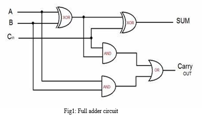
Full adder is a combinational circuit with 3 inputs. The primary 2 inputs are A and B, the third input Cin represents the carry. The two outputs are selected by the Sum (S) and Carry (C). Sum gives the values of least significant bit and Carry gives values of most significant bits. A pair of XOR gates, a pair of NAND gates and one OR circuit the full adder circuit is built.

II. EXISTING SYSTEM
Since the year 2000, portable electronic devices have been present everywhere in all the daily applications. Due to the reduced size and cost per device, these devices have grown into more numbers and have become more penetrable into users. Few frequently utilized examples include such as personal digital assistants, core mini-speakers, paging devices pocketalk language translator, Bluetooth key finder, Wi-Fi hotspot devices, hearing aids, smart health trackers, mobiles, laptops and tyre inflators etc. and many more. The electronic portable devices need to operate with reduced currents for achieving long battery duration.
Milad Jalalian Abbasi Morad, et al. proposed a design of new high-performance full adder using hybrid-CMOS logic style for high-speed applications. As The main structure of 1-bit full adder introduced in section 2. As mentioned in the previous section, the proposed full adder stands on third category. HSpice simulations using 65nm technology with a power supply of 1.2V was utilized to evaluate the performance of the seven circuits. To simulate a real environment, input buffers for all inputs of the test circuit are used. The transistor sizes of these buffers are chosen such that there is sufficient signal distortion as expected in an actual circuit. A minimum output load of fan-out of four inverters (FO4) is used for power and delay measurements (Goel et al., 2006), the value of which amounts to 1.234fF (about 0.308fF for each inverter in 65nm technology).
Nakul C. Kubsad et al., proposed a simulation and analysis of different CMOS full adders for delay optimisation. The expression is translated into complementary CMOS circuit to implement the traditional full adder. The design has NMOS and PMOS transistors that represents Pull down and pull up parts respectively. The implementation offers smart driving capability and full swing in output voltage. However because the semiconductor unit numbers are additional, it consumes additional power and occupied additional space. Because of several leakages, the sub threshold will increase. Because the pull up network consists of PMOS networks it ends up in high input capacitance and ends up in additional dynamic power and delay.
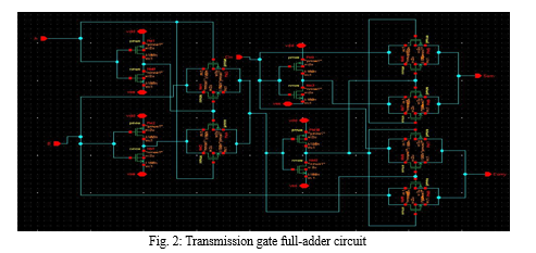
Transmission gate full adder circuit consists of twenty transistors to implement. Figure 3 represents the semiconductor unit level implementation of this topology. The design uses the XOR gates that is formed by transmission gate. A PMOS and an NMOS transistor are connected in parallel to create the transmission gate with control signals. Since transmission gate passes entire voltage vary at its output, therefore the degradation of output voltage of the adder is incredibly less. Parasitic Capacitance is accumulated because of the rise within the internal node count. The driving capability is lower when compared to alternative style methodologies. This circuit occupies less area than conventional circuit.
Aneela Achu Mathew et al. proposed a Comparative analysis of full adder circuits. The proposed full adder includes basically two functions, two EX-OR operation and MUX operation. In GDI, to perform EX-OR four transistors are required, and four MUX two transistors are needed. As the total transistors required is less, the power consumption has also decreased. The area needed is less. The analysis is done using Mentor Graphics Pyxis Version 10.1 Tool. It is done 180nm technology. Therefore, L is taken as 0.18u and width for PMOS is 0.9u, NMOS is 0.36u. Kavitha Khare et al. proposed a design a 1bit low power full adder using cadence tool. The proposed full adder circuit implement using NAND, NOR and Majority NOT gates. These gates are designed by using a simple inverter and MOS capacitance. To change threshold voltage of PMOS and NMOS of the inverter it works as NAND, NOR and majority NOT gates. The circuit shown in Fig.4 is works as a universal circuit. The NAND gate implement NMOS transistor at higher threshold voltage level and PMOS transistor at low threshold voltage level. For implement the NOR gate PMOS at high threshold voltage level and NMOS at low threshold voltage. For implement the majority NOT function both transistors are at high voltage level. Jakkula Gayathri et al., proposed a implementation and analysis of 6T 1bit full adder using cadence virtuoso. In Low power VLSI the primary design constraint is power consumption. Low power design plays an important role in high performance systems, as excessive power dissipation decreases the reliability and cost increases the expenditure in setting up the cooling system. Full adder is a basic building block of on chip libraries. It is a combinational circuit and finds applications in various digital circuits. These are used in processors, ALU and other computing devices. As a part of processors these are also used in calculating address, table indices etc. It adds two binary 1 bit digits along with carry in and produces sum and carryout.
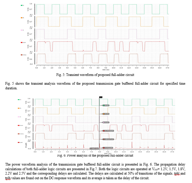
Chippe Keerthi et al., proposed a both the CMOS adder circuit’s i.e. conventional full-adder and proposed transmission gate full-adder circuit are designed, implemented and simulated in cadence virtuoso tool in 90nm process technology. The delays are calculated at 50% of transitions of the signals. tphl and tplh values are found out on the DC response waveform and its average is taken as the delay of the circuit. From the results it is revealed that the proposed full-adder circuit offers less delay as compared to the previous adder logics.
III. PROPOSED SYSTEM

The static CMOS full-adder circuit is the most popular and fundamental adder logic circuit which has robust features with respect to scaling of transistor dimensions, operating voltages, and process parameters. Power dissipation is also a concern in this logic circuit. For compensation against stability problems, extra buffer circuits are necessary. These shortcomings are overcome by using the proposed Transmission gate buffered CMOS full-adder logic circuit shown in the Fig. 2. It utilizes additional buffers for enhancing the driving capability and increasing the fan-out of the the digital circuit. The required transistor count for implementing this transmission gate CMOS full-adder logic circuit is only 20 as compared to 28 transistor count incase of conventional full-adder circuit. The proposed circuit offers buffered data outputs for corresponding data changes at the input side. Circuit designers make a trade-off approach in designing transmission gae based full-adder circuits with respect to higher operating speed, less die area and reduced power dissipation.


Conclusion
This paper describes the design, simulation and comparison of conventional CMOS full-adder and proposed transmission gate buffered full-adder logic circuit. The entire design and simulation is carried out in cadence virtuoso tool in 90nm process technology at a power supply voltage of 1.5V at a temperature of 25°C. To implement the sum and carry logic functions, the conventional CMOS full-adder logic circuit requires a transistor count of 28; whereas the transmission gate buffered full-adder logic required a transistor count of 20. The proposed circuit requires less number of transistors and nodes. Due to this it resulted in reduced switching activity, glitches and reduced wiring, which in turn led to low circuit area. By comparing both the full-adder logic circuits, it was observed that the transmission gate buffered full-adder logic circuit offered a 45 percent reduction in speed-power product.
References
[1] Parhami, B.: ‘Efficient hamming weight comparators for binary vectors based on accumulative and up/down parallel counters’, IEEE Trans. Circuits Syst., 2009, 56, (2), pp. 167–171 . [2] Liu, H.J.R., Yao, H.: ‘High-performance VLSI signal processing innovative architectures and algorithms’ (IEEE Press, Piscataway, NJ, 1998) . [3] Sheng, Y., Wang, W.: ‘Design and implementation of compression algorithm comparator for digital image processing on component’. Proc. Ninth Int. Conf. Young Computer Scientists, Hunan, China, November 2008, pp. 1337– 1341. [4] Abramovici, M., Breuer, M.A., Friedman, A.D., et al.: ‘Digital systems testing and testable design’ (IEEE Press, Piscataway, NJ, 1990). [5] Chan, A., Roberts, G.W.: ‘A jitter characterization system using a component in variant Vernier delay line’, IEEE Trans. Very Large Scale Integr. (VLSI) Syst., 2004, 12, (1), pp. 79–86. [6] Oklobdzija, V.G.: ‘An algorithmic and novel design of a leading zero detector circuit: comparison with logic synthesis’, IEEE Trans. Very Large Scale Integr. (VLSI) Syst., 1994, 2, (1), pp. 124–128 . [7] Suzuki, H., Kim, C.H., Roy, K., et al.: ‘Fast tag comparator using diode partitioned domino for 64 bit microprocessor’, IEEE Trans. Circuits Syst. I, 2007, 54, (2), pp. 322– 328. [8] Aguirre Hernandez.M et al., \\\"CMOS Full-Adders for Energy-Efficient Arithmetic Applications,\\\" IEEE Trans. on Very Large Scale Integ. Systs., vol. 19, no. 4, pp.(718-721), April 2011. [9] Murshed.A.M. et al., \\\"A 10-bit high speed pipelined ADC,\\\" Second Intern. Conf. on Inv. Sysms. and Control (ICISC), Coimbatore, India, 2018, pp. (1253-1258). [10] Giustolisi.G et al., “Analysis and Comparison in the Energy-Delay Space of Nanometer CMOS One-Bit Full-Adders,\\\" IEEE Access Journal, vol. 10, pp. (75482-75494), 2022. [11] K. S. Kumar et al., \\\"A High Speed Flash Analog to Digital Converter,\\\" Second International Conference on I-SMAC (IoT in Social, Mobile, Analytics and Cloud) (I-SMAC),Tamil Nadu, India, 2018, pp. (283-288). [12] K. L. Krishna et a., \\\"A 1V second order delta sigma ADC in 130nm CMOS,\\\" International Conference on Information Communication and Embedded Systems (ICICES2014), Chennai, India, 2014, pp. 1-5. [13] A. Parthipan et al., \\\"A High Performance CMOS Operational Amplifier,\\\" 2019 3rd International Conference on Computing Methodologies and Communication (ICCMC), Erode, India, 2019, pp. 702-706. [14] Krishna, K.L., Al-Naamani, Y.M.A., Anuradha, K. (2018). A High Speed Two Step Flash ADC. In: Zelinka, I., Senkerik, R., Panda, G., Lekshmi Kanthan, P. (eds) Soft Computing Systems. ICSCS 2018. Communications in Computer and Information Science, vol 837. Springer, Singapore.
Copyright
Copyright © 2024 J. Ganesh Reddy, J. Priyanka Keerthi, K. Revanth, K. Sai Deekshitha, K. Upendra Raju. This is an open access article distributed under the Creative Commons Attribution License, which permits unrestricted use, distribution, and reproduction in any medium, provided the original work is properly cited.

Download Paper
Paper Id : IJRASET58352
Publish Date : 2024-02-08
ISSN : 2321-9653
Publisher Name : IJRASET
DOI Link : Click Here
 Submit Paper Online

