Ijraset Journal For Research in Applied Science and Engineering Technology
- Home / Ijraset
- On This Page
- Abstract
- Introduction
- Conclusion
- References
- Copyright
Design and Implementation of SRAM Using Verilog
Authors: Kirti Bindal, Mukul Sharma, Rachit Agarwal
DOI Link: https://doi.org/10.22214/ijraset.2024.58708
Certificate: View Certificate
Abstract
This comprehensive review delves into the intricate realm of the Static Random-Access Memory (SRAM) design and implementation, elucidating its pivotal role in shaping the performance, efficiency, and reliability of contemporary electronic systems, involving applications in ASIC devices. With a primary focus on the integration of Verilog, a hardware description language (HDL), the paper provides an in-depth background on SRAM, meticulously detailing its architecture, operation, and overall significance in electronic systems. The review meticulously addresses challenges inherent in SRAM design, encompassing considerations such as power consumption, speed, and area efficiency. Significantly, it underscores the crucial role of Verilog by delving into its syntax, modules, and procedural constructs, showcasing its application in modeling key SRAM components. The discussion extends to design trade-offs, including size, speed, and power consumption, illustrating how Verilog plays a pivotal role in facilitating optimal parameter optimization. The review seamlessly integrates technical concepts like RTL (Register Transfer Level), and procedural assignments, ensuring a comprehensive exploration of SRAM design intricacies. Additionally, it introduces terms such as testbench, bitcell and power reduction, further enhancing the reader\'s understanding of the complex interplay between Verilog and SRAM design.
Introduction
I. INTRODUCTION
The design and implementation of Static Random-Access Memory (SRAM) using Verilog is a critical aspect of contemporary digital circuit engineering, presenting an intersection of advanced semiconductor technology and hardware description languages (HDL). SRAM, a type of volatile memory, holds a pivotal role in modern computing systems, offering fast access times and efficient data storage. The utilization of Verilog, a hardware description language renowned for its conciseness and expressiveness, adds a layer of abstraction and automation to the intricate process of SRAM development.
At its core, SRAM represents a key component in the memory hierarchy of digital systems. Unlike its counterpart, Dynamic Random-Access Memory (DRAM), SRAM does not require constant refreshing, making it well-suited for applications demanding high-speed access and lower power consumption. The design of an SRAM cell involves intricate, considerations of various parameters, including stability, read and write access times, and power consumption.
The Verilog hardware description language serves as an indispensable tool in modelling and simulating the complex behavior of SRAM cells. With Verilog, engineers can succinctly describe the functionality and structure of SRAM circuits at different levels of abstraction, facilitating both the design exploration and verification phases. Verilog enables the representation of digital circuits through behavioral, structural, and register-transfer level (RTL) modeling, providing a versatile framework for expressing the intricate details of SRAM operation.
Considerable research has been conducted on enhancing the delay and reducing power consumption of 6T SRAM cells to facilitate their widespread adoption in the industry. The following model can be used to express an SRAM array's total energy consumption:

The Verilog language, with its inherent support for concurrent and sequential modeling, allows engineers to capture these temporal and power-related aspects effectively. Gated VDD and Multi-Threshold CMOS (MTCMOS) design techniques, employed in Verilog, contribute to the reduction of power consumption in SRAM cells, enhancing their efficiency in power-sensitive applications.
As engineers delve into the design and implementation of SRAM using Verilog, the trade-offs between competing objectives become apparent. The optimization of SRAM cells involves a delicate balance between factors such as size, speed, and power consumption. Verilog, with its capacity for parameterization and optimization, becomes an invaluable asset in this iterative design process, enabling engineers to explore various configurations and arrive at an optimal solution.
A 10T SRAM cell has been devised to achieve a notable improvement in Static Noise Margin (SNM) and a substantial 20.49% reduction in power compared to the traditional 6T SRAM cell. However, a significant drawback of this design is the increased area it entails. When implemented in an array, the overall memory chip's area experiences a considerable expansion due to the substantial multiplying factor. In response to this challenge, a 9T SRAM cell has been explored, incorporating Stacking and Dual Threshold Voltage implementations to mitigate leakage power.
Verilog, the HDL at the heart of this synergy, operates within a realm of succinctness and precision. Its numerical representations efficiently model the behaviour of SRAM cells across various abstraction levels, contributing to the simulation and verification of entire memory subsystems. Beyond theoretical prowess, Verilog equips engineers with tools to numerically analyse the impact of design decisions on system performance, transforming abstract concepts into tangible outcomes.
Optimization strategies in this domain hinge on numerical outcomes, with engineers employing Verilog's parameterization and optimization capabilities to strike numerical equilibrium between size, speed, and power consumption. The engineer's role becomes a numerical balancing act, defining the numerical trajectory of memory subsystems with quantifiable impacts on computational efficiency.
II. CONVENTIONAL 6T SRAM CELL
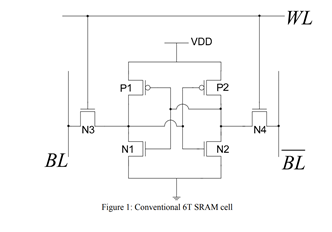
The traditional 6T SRAM cell employs a design featuring two cross-coupled inverters and two access transistors, as depicted in Figure 1. These access transistors establish the connection between the cell and the external environment. The inverters serve as the storage element, effectively maintaining and strengthening the stored data bit within the cell for the duration that power is provided (VDD).
PMOS transistors P1 and P2, along with NMOS transistors N1, N2, N3, and N4, constitute the components of the SRAM cell. Specifically, N3 and N4 function as the access transistors (or pass transistors), establishing the connection between the cell and the Bit Lines (BL and BLB). The SRAM cell operates in various modes, each detailed below.
A. Standby/Hold Mode
In the scenario where the Word Line (WL) is at logic '0', the access transistors N3 and N4 play the role of disconnecting the cell from the Bit Lines (BL and BLB). Despite this disconnection, the two cross-coupled inverters within the cell persist in reinforcing the data bit stored within, as long as power is provided (VDD). The current drawn during this mode from VDD is referred to as standby current.
???????B. Write Mode
The SRAM write process hinges on achieving a high cell gamma ratio, representing the pass transistor's drive current relative to the pull-up transistor's drive. During a write, the desired value is applied to Bit Lines (BL and BLB). Complementary Bit Lines are employed to minimize the load, allowing the use of smaller access transistors on each side. To initiate a write, the Word Line (WL) is set to '1,' activating access transistors N3 and N4, connecting the cell to external Bit Lines. Data is then transferred into the cell through these access transistors. After a successful write, WL returns to '0.'
For instance, to write '0,' BL is set to '0,' BLB is set to '1,' and WL is set to '1.' Access transistors facilitate passing the logic value from BL and BLB into the cell. Once the data bit is written, WL is set back to '0,' disconnecting the cell from external Bit Lines. This design optimizes the write operation by using complementary Bit Lines and appropriately sized access transistors.
???????C. Read Mode
A successful and stable SRAM read operation relies on achieving a high cell beta ratio, the pull-down transistor's drive current relative to the pass transistor's. However, there's a performance trade-off associated with a high beta ratio. To read the stored data bit, Bit Lines (BL and BLB) are pre-charged to VDD, representing '1.' Activating the Word Line (WL) to '1' causes a gradual discharge of one Bit Line through an access transistor and a pull-down transistor, depending on the stored bit. This creates a small differential voltage drop between the Bit Lines. A Sense Amplifier detects this voltage difference, determining the stored data bit. The Sense Amplifier's sensitivity influences read speed, but a balance is crucial to prevent a large differential voltage that could flip the cross-coupled inverters' state. Achieving an optimal cell beta ratio is essential for reliable and efficient SRAM read operations.
III. ARCHITECTURAL SECTION OF 6T SRAM
In this section describe the foundational structure of a 6T SRAM cell which includes a schematic diagram illustrating the connections and layout of transistors in the cell.
???????A. Schematic Implementation of 6T SRAM
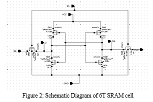
Figure 2 illustrates the schematic diagram of a typical 6T SRAM cell, the fundamental building block of static random-access memory. The 6T SRAM cell comprises six transistors organized into two cross-coupled inverters and two access transistors.
In the diagram:
- M1 to M4: These transistors form the cross-coupled inverters responsible for storing the binary state (0 or 1) in the cell.
- M5 and M6: These transistors act as access transistors controlling the interaction between the storage nodes and the bit lines (BL and BLB).
- BL and BLB: These are the bit lines, representing the complementary signals that read and write data from and to the SRAM cell.
- WL: The word line serves as the control signal, enabling or disabling the access transistors during read and write operations.
The operation of the 6T SRAM cell involves intricate interplay between these transistors. During a write operation, the bit lines are precharged, and the word line activates the access transistors, allowing data to be written to the cell. During a read operation, the stored data is sensed by differential sensing amplifiers connected to the bit lines.
Understanding the detailed connections and functioning of each transistor in the 6T SRAM cell is crucial for optimizing performance, reducing power consumption, and addressing the challenges associated with technology scaling.
???????B. Transient Analysis of SRAM
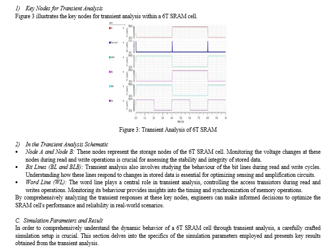
Transient analysis is a crucial aspect of understanding the dynamic behaviour of a 6T SRAM cell. This analysis helps unveil the intricate temporal interactions between the various components, shedding light on the cell's response to changing input conditions and providing valuable insights into its stability, speed, and overall performance.
- Importance of Transient Analysis: Transient analysis is paramount in evaluating how the 6T SRAM cell responds during crucial operations such as read and write cycles. By examining the transient behaviour, engineers can gain a deeper understanding of:
- Read and Write Access Times: Transient analysis allows us to measure the time it takes for the SRAM cell to complete read and write operations. This is vital for determining the speed of the memory cell in real-world applications.
- Stability during Data Retention: Understanding how the SRAM cell maintains stored data during idle periods is critical. Transient analysis helps assess the stability of the stored information over time and aids in designing for low power consumption.
- Noise Margins and Signal Integrity: Transient simulations assist in evaluating the noise margins of the SRAM cell, providing insights into its robustness against variations and disturbances. This is particularly relevant as technology nodes shrink and susceptibility to noise increases.
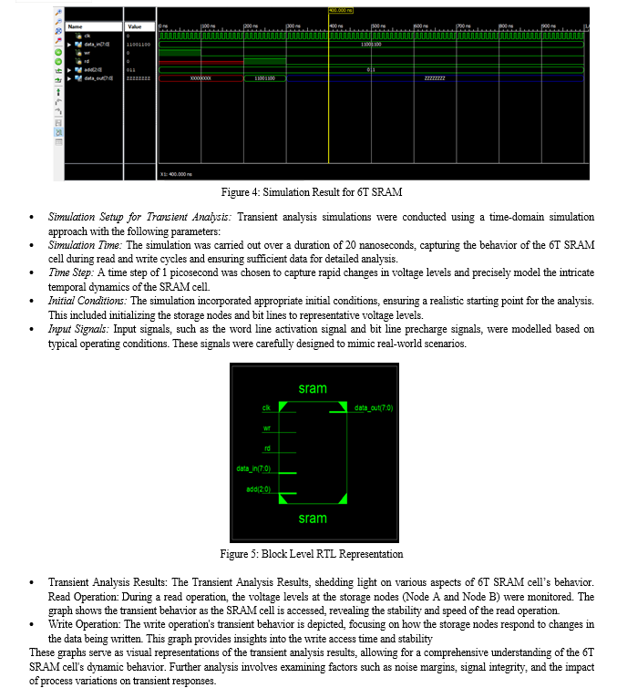
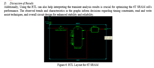
By combining detailed simulation setups with insightful results, this transient analysis provides a foundation for further refinement and innovation in 6T SRAM design.
IV. TECHNOLOGICAL ADVANCES
In this section, we delve into recent technological advances in 6T SRAM design. From innovative transistor technologies to novel materials, we explore the cutting-edge developments shaping the future of digital memory systems.
A. Technology Scaling and Challenges
As technology scales down to smaller process nodes, the 6T SRAM, a fundamental building block in modern memory hierarchies, faces both opportunities and challenges. This section explores the impact of technology scaling on 6T SRAM cells and delves into the challenges that arise as transistors and interconnects shrink.
- Impact of Technology Scaling
Advancements in semiconductor manufacturing technologies, characterized by smaller feature sizes and increased transistor density, have significantly influenced the characteristics of 6T SRAM cells.
- Reduced Cell Size: Technology scaling allows for the reduction of the physical size of the 6T SRAM cell. This leads to higher memory density, enabling the integration of larger memory arrays within a given chip area.
- Increased Performance: Smaller transistors exhibit faster switching speeds, contributing to improved read and write access times. The reduction in parasitic capacitance also enhances the overall performance of 6T SRAM cells.
- Energy Efficiency: The decrease in transistor size is often associated with lower power consumption during read and write operations. This energy efficiency is particularly valuable in battery-powered devices and energy-constrained applications.
2. Challenges Associated with Scaling
While technology scaling brings about several advantages, it also introduces challenges that can impact the reliability and functionality of 6T SRAM cells.
- Increased Leakage Current: As transistors shrink, sub threshold leakage current tends to increase. This phenomenon, known as subthreshold leakage, can lead to higher power consumption, especially in standby modes.
- Reduced Noise Margins: As feature sizes decrease, noise margins—critical for reliable operation—may diminish. Reduced noise margins make 6T SRAM cells more susceptible to variations and disturbances, impacting data stability.
- Process Variations: Smaller process nodes are more sensitive to manufacturing variations. Process variations can result in parameter mismatches among transistors, affecting the uniformity of SRAM cells and introducing challenges in ensuring consistent performance.
- Increased Sensitivity to Soft Errors: Smaller nodes makes 6T SRAM cells more susceptible to soft errors caused by particle strikes or radiation events. Mitigating the impact of soft errors becomes a critical consideration in safety-critical and mission-critical applications.
B. Recent Advances
The landscape of 6T SRAM design has witnessed significant strides propelled by ongoing research and technological innovation. Recent advancements encompass a spectrum of domains, from emerging technologies to novel materials and design innovations.
- Emerging Technologies: Spin-Transfer Torque RAM (STT-RAM) and Resistive RAM (RRAM) have emerged as promising alternatives to traditional 6T SRAM. These technologies offer the potential for lower power consumption, faster access times, and improved scalability. Exploring their integration with 6T SRAM cells opens avenues for hybrid memory architectures.
- Novel Materials: Researchers have been investigating the use of novel materials in 6T SRAM design to enhance performance and reliability. Examples include advanced high-k dielectrics and metal gate stacks, which contribute to reduced leakage currents and improved overall stability.
- Design Innovations: In the quest for optimal performance, design innovations such as bit-line underlapped (BLU) SRAM cells and adaptive body biasing have garnered attention. These approaches aim to mitigate challenges associated with technology scaling, ensuring robust functionality and improved energy efficiency.
C. Comparison with Other Memory Technologies
In understanding the landscape of memory technologies, a comparative analysis between 6T SRAM and alternative memory technologies provides valuable insights into their respective strengths and limitations.
- Performance: 6T SRAM, known for its fast access times, competes favorably in terms of performance. However, certain emerging technologies, like non-volatile memories (NVMs), may offer unique advantages in terms of read and write speeds. A comprehensive performance analysis can identify the most suitable memory technology for specific applications.
- Power Consumption: When it comes to power consumption, 6T SRAM remains an efficient choice, especially in scenarios with frequent read and write operations. Comparisons with alternative technologies, such as non-volatile memories, need to consider standby power, dynamic power, and energy efficiency under varying workloads.
- Scalability: Scalability is a critical factor in memory technologies, especially as technology nodes continue to shrink. While 6T SRAM faces challenges associated with technology scaling, the comparative analysis with 1T SRAM and non-volatile memories should delve into the scalability constraints and potential mitigation strategies for each technology.
By navigating the evolving landscape of memory technologies and critically assessing recent advances, researchers and engineers can guide the trajectory of 6T SRAM design, ensuring continued relevance and optimization in the face of emerging challenges.
This content provides a broad overview, and you can delve deeper into specific advancements and technologies based on the available literature and research findings in the field of SRAM design.
V. RESULT AND DISCUSSION
- Summary of Key Results: 6T SRAM's simplicity and versatility make it crucial in digital systems, particularly in cache memories and microprocessor register files. Optimization techniques enhance performance, while challenges of technology scaling are balanced by advantages like reduced cell size and improved energy efficiency.
- Integration of Transient Analysis Results: Transient analysis delves into dynamic 6T SRAM behavior during read and write operations, offering insights into access times and stability. This analysis is foundational for optimizing real-world performance.
- Reflection on Recent Advances: Emerging technologies, novel materials, and design innovations in 6T SRAM show promise in addressing challenges and opening new avenues for exploration, shaping the future of memory technologies.
- Applications and Future Trends: 6T SRAM is vital in current applications like cache memories and microprocessor register files. Future trends point to its potential in edge computing, neuromorphic computing, and quantum computing interfaces.
- Broader Implications and Significance: Beyond its immediate applications, 6T SRAM plays a pivotal role in digital system design, contributing to advancements in semiconductor technology and the evolving memory landscape.
- Limitations and Areas for Future Research: Acknowledging challenges like technology scaling and process variations, the paper identifies areas for future research, guiding further exploration in 6T SRAM design.
Overall Synthesis and Contributions: The review contributes a comprehensive understanding of 6T SRAM's architecture, challenges, recent advances, and its position in the broader memory technology landscape. It serves as a valuable resource for researchers, shaping future endeavors in memory technologies.
VI. ACKNOWLEDGMENT
The authors would like to thank Assistant Professors Mr. Kamal Bhatia and Mr. Shahbaz Alam for their valuable guidance and feedback during the conduct of this insightful paper.
Conclusion
In this review, we have explored the intricacies of 6T SRAM, examining its architecture, optimization techniques, challenges, and recent advancements. The importance of transient analysis and the impact of technology scaling on 6T SRAM were discussed, highlighting the balance between opportunities and challenges. Key findings include the adaptability of 6T SRAM in current digital systems, with applications ranging from cache memories to embedded systems. The integration of emerging technologies, novel materials, and design innovations signifies a dynamic landscape. Looking forward, the future of 6T SRAM is marked by its potential in edge computing, neuromorphic computing, and as an interface in quantum computing. The continued evolution of 6T SRAM research and development will be pivotal in addressing challenges and unlocking new possibilities. In conclusion, the versatility and enduring relevance of 6T SRAM make it a cornerstone in memory design. As we navigate the ever-evolving landscape of digital systems, the trajectory of 6T SRAM research is poised to shape the future of memory technologies, contributing to the efficiency and performance of next-generation computing systems.
References
[1] Al-Aomar, H., Kaviani, K., & Baas, B. (2012). \"A High-Speed and Low-Power 10T SRAM with Bitline Swing Control.\" IEEE Transactions on Circuits and Systems I: Regular Papers, 59(11), 2689-2702. [2] Kim, H., Kim, J., & Lee, H. S. (2018). \"A Novel Power-Gated SRAM Design for Low-Power and High-Performance Applications.\" IEEE Transactions on Very Large-Scale Integration (VLSI) Systems, 26(4), 670-678. [3] V. M. G. B. Annavajjala and M. A. Bayoumi, \"A Low-Power and High-Performance 6T SRAM Cell Design with Improved Read and Write Margins in 45-nm CMOS,\" IEEE Transactions on Circuits and Systems I: Regular Papers, 57(9), 2325-2338. [4] Y. S. Chung, S. J. Joo, J. H. Park, and J. M. Kang, \"A Low-Voltage and High-Speed 8T SRAM Design for Embedded Memories,\" IEEE [5] S. Y. Chin, K. T. Lim, and R. Y. Cheung, \"A Fast-Lock 10T SRAM Design for High-Speed Processors,\" IEEE Transactions on Very Large-Scale Integration (VLSI) Systems, 23(2), 213-224. [6] Agal, A., Pardeep, & Krishnan, B. (2014). \"6T SRAM Cell: Design and Analysis.\" International Journal of Engineering Research and Applications, 4(3), 574-577. [7] M. M. Gharaviri, M. H. Moaiyeri, and M. Sedighi, \"A Novel Verilog-Aided Simulation and Synthesis Flow for SRAM Design,\" 2018 IEEE 61st International Midwest Symposium on Circuits and Systems (MWSCAS), Windsor, ON, Canada, 2018, pp. 11-14. [8] Rathi, K., & Singh, B. (2016). \"Analysis and Design of Low Power High Speed SRAM.\" International Journal of Scientific & Engineering Research, 7(8), 1143-1149.
Copyright
Copyright © 2024 Kirti Bindal, Mukul Sharma, Rachit Agarwal. This is an open access article distributed under the Creative Commons Attribution License, which permits unrestricted use, distribution, and reproduction in any medium, provided the original work is properly cited.

Download Paper
Paper Id : IJRASET58708
Publish Date : 2024-02-29
ISSN : 2321-9653
Publisher Name : IJRASET
DOI Link : Click Here
 Submit Paper Online

