Ijraset Journal For Research in Applied Science and Engineering Technology
- Home / Ijraset
- On This Page
- Abstract
- Introduction
- Conclusion
- References
- Copyright
Design of High Performance Core Micro-Architecture Based on RISC-V ISA for Low Power Applications
Authors: Nidhi Jaiswal
DOI Link: https://doi.org/10.22214/ijraset.2023.54647
Certificate: View Certificate
Abstract
Numerous current and future applications aim to create highly efficient central processing units (CPUs). The RISC V processor micro-architecture is one illustration of a design that satisfies the necessities. The RISC-V Instruction Set Architecture [ISA] provides support for the micro-architecture. The instruction set architecture and the micro-architecture of a processor are two of the most crucial aspects of its design. The multiplier and divider circuits have a relatively high level of hardware complexity compared to other stages of the instruction execution process, which must be taken into account in any core micro-architecture. The construction of an appropriate hardware circuit that is capable of multiplication and division determines the overall size, power, and performance of a core. This center has four phases, and during those stages, each guidance is done, except for stacking and putting away information. The arithmetic operations can be completed within one clock cycle. On the other hand, the division and multiplication operations are repeated in an effort to shorten the critical path latency.
Introduction
I. INTRODUCTION
Diminished Guidance Set PCs (RISCs) are currently use for all sort of computational errands.
RISC workstations are increasingly being utilized for compute tasks such as DSP, DIP, and others in the field of scientific computing. When compared to other systems, RISC concepts assist in achieving specified levels of performance at significantly lower costs. RISC-based plans will keep on filling in speed and limit, and pipelined RISC further creates speed and cost sufficiency over the straightforwardness of gear depiction language programming and memory assurance. The ability to hardwire the instruction set to accelerate instruction execution is one of the RISC processor's primary features. The design of a Reduced Instruction Set Computer (RISC) processor with a data width of four bits is presented in this work. It has a simple arithmetic logical unit (ALU) for basic operations, memory for programs and data, general-purpose registers, and a comprehensive instruction set. The majority of the instructions in this design are the same length and structure, arithmetic operations can only be performed in CPU registers, and load and store instructions can access memory separately. To assist with activities like number juggling, coherent, moving, and load-store, the engineering follows eight directions. A typical language for depicting equipment is Verilog HDL. A language used to illustrate a computerized framework is referred to as "equipment illustrative language." HDLs enable architectural experimentation and error correction by enabling design simulation earlier in the design cycle. HDL plans are innovation independent, simple to plan and investigate, and typically easier to read than schematics, especially for large circuits. All the more as of late Verilog is utilized as a contribution for combination programs which will create an entryway level portrayal for the circuit. Xilinx ISE and Model sim serve as the language's simulator. Verilog can convey straightforward behavior. The processor is able to handle multiple instructions at once thanks to machine cycle instructions. The processor is able to operate at a high clock frequency, resulting in increased speed.
II. PROPOSED MODEL
The ability to speed up instruction execution is one of the RISC processor's main features. For single-cycle execution, there is no need for microcode. The length of each instruction is fixed in bits. This makes the guidance bring instrument simpler because the area of guidance limits is independent of the type of guidance. There are only a few address modes available to the processor. Memory can be accessed by load/store instructions only; They operate between memory and a register. The cycle time of the machine is reduced. The proper size of the guidelines permits the directions to be effectively funneled. The RISC architecture is adaptable and extensible, maximizing the performance of any semiconductor technology.
RISC incorporates augmentations to RISC ideas that assist with accomplishing given degrees of execution at essentially lower cost than different frameworks. The design process is quick and inexpensive. The majority of the instructions in this design are the same length and structure, arithmetic operations can only be performed in CPU registers, and load and store instructions can access memory separately. Specific bring, unravel, execute, and store are the four phases that make up the guidance cycle. The Control Unit generates signals for the selected Instruction following each instruction fetch. In order to facilitate arithmetic, logical, shifting, and load-store operations, the architecture supports eight instructions.
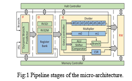
Let us take each stage of pipeline technique as,
- Cycle of Instructions Fetching (if)
After retrieving the current instruction from memory, put the program counter (PC) back into the memory. You can update the PC to the ensuing model by adding one.
2. Instructions for Decoding and Recording the fetch cycle's ID
Peruse the registers relating to enlist source specifiers from the register record and decipher the direction. Due to the RISC architecture's fixed location of the register specifiers, decoding can be performed concurrently with reading registers. Fixed-field decoding is the name given to this method.
3. (EX) Execution
Depending on the type of direction, the ALU performs one of three tasks on the organized operands from the previous cycle. Instructions for the ALU Register: The ALU performs the action specified by the ALU opcode on the qualities of the register record.
4. Store result (ST)
Instructions for the register-register ALU or load: Create the result into the register record, regardless of whether it comes from the ALU (for an ALU direction) or the memory system (for a pile).
III. BRANCH AND DYNAMIC PREDICTOR
A. Expectation of the Branch
- The presence of program transfer instructions like JMP, CALL, RET, and others can reduce pipeline gains.
- These instructions change the order, making all instructions that followed instructions for program transfer invalid.
- Consequently, while the pipeline stages are reloaded, no work is performed.
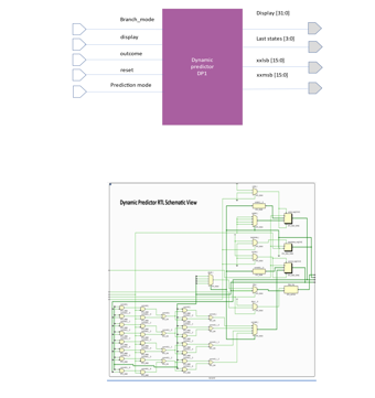
Predictive logic for branches: To avoid this problem, Pentium employs the Powerful Branch Expectation strategy. A prediction about the branch instruction that is currently in the pipeline is made in this scheme. The expectation will either work out or not. Neither the clock cycles nor the pipeline will be flushed if the prediction is correct. The pipeline is flushed and restarted with the current instruction if the prediction is incorrect. A related store with 256 passages and 256 different ways is utilized in its execution. Branch Target Buffer (BTB) is the name of this. The following information can be found in each line's directory entry:
Good bit: Demonstrates regardless of whether the section is legitimate.
Section on history: Keep track of the quantity of chomped consumed.
The place where the branch guidance was obtained is the location of the source memory. Assuming the catalog passage is certified, the comparing information section in BTB stores the branch's objective location.
B. Prediction of Branch Function
- BTB is a lookaside cache that looks for branch instructions by monitoring the Decode Instruction (DI) stage of two pipelines.
- The BTB plays out a hold question in its source memory the underlying time a branch direction enters the pipeline.
- Since the guidance has never been seen, it is a BTB mistake. Despite being an unconditional jump instruction, it predicts that the branch will not be taken.
- The branch will be taken or not when the instruction reaches the EU (execution unit).The branch target address will be used to retrieve the next to be executed instruction if it is taken. Instructions will be retrieved sequentially if not taken.
- The execution unit provides feedback to the branch prediction whenever a new branch is taken. The returned address of the branch target is recorded in BTB.
The source memory address is set into an inventory, and the arrangement of encounters digit is set to immovably taken.
The advantages of improved execution brought about by branch prediction: By anticipating the outcome of restrictive branches, the Pentium is able to recover and carry out the instructions in the anticipated manner while avoiding the presentation penalty that is associated with incorrectly anticipated branches enhanced directional viability: By allowing the processor to continue fetching and executing instructions from the predicted path while waiting for the results of earlier instructions, branch prediction enables the Pentium to maintain a high instruction throughput. Reduced punishment for making an incorrect prediction of the branch: The Pentium's dynamic branch expectation component is capable of rapidly adapting to changes in program behavior, lowering the penalty for branch mispredictions.
C. RISC Instruction Decoder
The RISC machine keeps instruction execution extremely quick and straightforward. Thusly, the course decoder, for example, there is one should be all around as smoothed out as could really be expected. The more complex machine functions necessitate the execution of additional instructions. The machine code compiler must provide every low-level abstraction.
A RISC decoder typically comes in two varieties because the pieces of the guidance code are simply transferred to the equipment components, the initial version has no decoder at all. A guidance decoder cannot delay execution; the machine code must be meticulously modified to meet all timing requirements. The sequence of instructions directly generates the required "waveforms" for the control line. The hardware begins to respond as soon as the instruction is given. The guidance set's components address the actual controls of the equipment parts in a straightforward manner.
A clear and quick decoder links the hardware components and the direction code in the following form. Typically, discrete reasoning entrances are used to complete this interpretation. This decoder's primary objective is to produce a "cleaner" representation of the guidance set. Even though using a decoder frequently reduces the number of bits required in the machine code word, each instruction still represents a single machine function, just like in the direct variant. Consequently, this may be able to launch multiple equipment capabilities from a single machine guidance.
After retrieving the subsequent instruction from memory, the Instruction Decoder sends its individual instructions to the appropriate locations. The control unit on each control signal line creates the heartbeat sequence necessary to carry out (and obtain) each machine-language guidance.
A pipeline register interfaces the control store ROM's all's result pieces each clock cycle.
The pipeline register latches a new set of bits with each clock cycle.
The sequencer produces two sections: control bits that communicate with the processor's hardware components. the "microPC" that is related with a piece of the control store ROM's area inputs. The pass pennant may be included in one of the area commitments made by the control store ROM, according to some.

IV. PROGRAM COUNTER
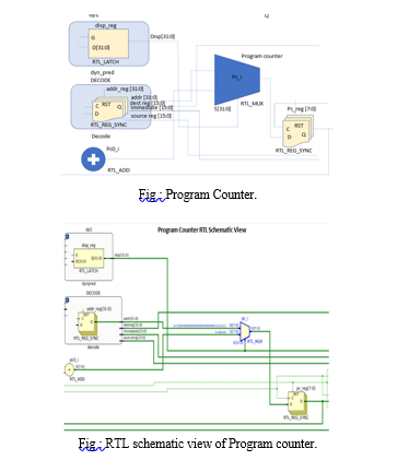
A register known as the Program Counter, or PC, stores the new location added to the guidance memory. The location is introduced to guidance memory at the beginning of a cycle. The instruction is read from instruction memory during the cycle, and a calculation is performed simultaneously to select the subsequent PC.
RV32I provides a little-endian and byte-addressed 32-bit user address space"). Since each RV32 instruction is 4 bytes, it makes sense to think of the PC as incrementing by 4 when using byte addresses. At the point when we say RISC-V additions the PC by 4, this means for some random byte address X of a 32-cycle RISC-V guidance, the following guidance will start in memory at address X+4. ( Keep in mind that the PC is increased by 2 when compressed instructions are used (16 bits per 2 bytes).An IMEM read width of 16 pieces implies 2 peruses from IMEM are important to get a full guidance, and an IMEM read width of 32 pieces implies just 1 read from IMEM is important to get a full guidance. In any case, these are execution contemplations, not an ISA thought - you could speculatively carry out an ISA-agreeable RISC-V processor with one or the other kind of IMEM.
V. RISC-V INSTRUCTION MEMORY
A RISC CPU program has one memory for the LOAD and STORE instructions, as well as computational instructions like ADD, SUB MUL, and so on. have three addresses, each of which refers to processor registers
A. Processors with RISC
In order for their instructions to be executed in the CPU at a much faster rate with fewer references to memory, these processors have a simple addressing mode and a small instruction set.A processor of this kind is known as a RISC (reduced instruction set computer).
- The characteristics of the RISC processor are as follows: There are a lot of registers in their system.
- They accelerate technique call and return by utilizing covered register windows.
- Their pipeline of teachers is strong.
- They provide compiler support, making it simple to convert machine language programs into programs written in significant level dialects.
B. RISC Instructions
The LOAD and STORE instructions, which are used to communicate with the CPU and memory, make up the majority of a typical RISC processor instruction set.
The central processor's registers complete any leftover directions without alluding to the memory.
With a single memory and central processor register address, a RISC computer chip program includes computational instructions (such as ADD, SUB MUL, etc.) as well as burden and STORE instructions. have three locations, one for every processor register.
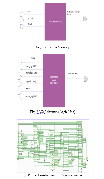
When performing arithmetic operations on operands, the Arithmetic Logic Unit (ALU) is utilized. These operands as a rule come from register document as well as guidelines. It performs a variety of arithmetic operations, including logical shift, addition, subtraction, and xor. ALU, which is also known as a "functional unit," has multiple arithmetic functionalities, as previously mentioned. ALU must select which functionality (addition, subtraction, logical shifting, etc.) to execute on each arithmetic-related instruction execution. This way of behaving of ALU is constrained by control signal discharged either by control unit or Guidance Decoder (relies upon execution). The ALU _in_ scl signal from Control until instructs ALU to select the Addition function in the preceding example. After ALU applied number juggling procedure on the operands, the outcomes are composed back to enlist document, in which rd signal pick which area of Register Record the outcome will be put away in.
VI. MULTIPLIER
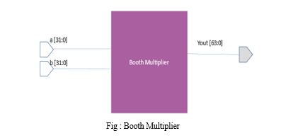
A. Booth Multiplication
Two signed binary numbers are multiplied using Booth's multiplication algorithm, which uses two's complement notation. Andrew Donald Booth developed the algorithm in 1950 while conducting research on crystallography.
B. Algorithm
Two signed binary numbers are multiplied using Booth's multiplication algorithm, which uses two's complement notation. Andrew Donald Booth developed the algorithm in 1950 while conducting research on crystallography.
VII. TYPICAL IMPLEMENTATION
Find the P and A initial values, as well as the A and S initial values; Booth's algorithm can be implemented by repeatedly adding one of two predetermined values A and S to a product P using ordinary unsigned binary addition, followed by a rightward arithmetic shift on P. The number of bits in m and r should be represented by x and y, and their lengths should all be the same as (x + y + 1).
A: Fill the most important bits (on the left) with the value of m and zero the remaining bits (y + 1)
S: In two's complement notation, enter the value of (m) into the most significant bits. Zero the (y + 1) bits that are left over.
P: Zeros should be used to fill in the most important x bits. Add the value of r to the right of this, and then zero the least significant (rightmost) bit.
2. Find the value of P + A if the two least significant (rightmost) bits of P are 01, and ignore any overflow.
Ignore any overflows and determine the value of P + S if they are 10.
Right shift if they are 00. In the subsequent step, directly use P.
Assuming they are 11, do right move. In the subsequent step, directly use P.
3. Numerically shift the worth got in the second step by a solitary spot to one side. P should now be equal to this new value.
4. Steps 2 and 3 should be carried out a total of y times.
5. Drop the most un-huge (furthest right) piece from P. This is the result of m and r.
VIII. APPLICATION OF A 3*2 MODIFIED WINOGRAD CONVOLUTION ALGORITHM
Using its pneumonic implementation, we have applied a 3*2 modified Winograd algorithm to describe the processor's functionality in relation to its use in signal processing applications.
The processor's instruction memory is where the respective opcodes are initially stored. The relevant data memory, which ought to extend beyond memory location 26 in this instance, houses the inputs. The maximum widths of the inputs x0, x1, and x2 are six bits, while the values of h0 and h1 are three bits.
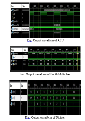
The program finishes after 26 clock cycles with the expected outcomes S0, S1, S2, and S3, showing the way that the processor can do single-cycle directions. Additionally, it demonstrates its application in a typical signal processing scenario. The MAC operation, which is frequently used in signal processing applications, can be carried out by repeatedly executing instructions for multiplication and addition. As a result, there would be no need for a separate MAC unit.
IX. RESULTS
Conclusion
The work focuses on the design and implementation of 32-bit ALU & incorporation the ALU in RISC V micro architecture processor and RISC V instruction set architecture ISA and comparing design metrics like Area, Power, Delay, Latency and Throughput.
References
[1] Waterman, Y. Lee, D. A. Patterson, and K. Asanovic, “The RISCV instruction set manual, volume I: User-level ISA, version 2.0,” EECS Dept., Univ. California at Berkeley, Berkeley, CA, USA, Rep. UCB/EECS-2014-54, May 2014. [Online]. [2] Available: http://www2.eecs. berkeley.edu/Pubs/TechRpts/2014/EECS-2014-54.html [3] Berkeley.edu/Pubs/Tech
Copyright
Copyright © 2023 Nidhi Jaiswal. This is an open access article distributed under the Creative Commons Attribution License, which permits unrestricted use, distribution, and reproduction in any medium, provided the original work is properly cited.

Download Paper
Paper Id : IJRASET54647
Publish Date : 2023-07-06
ISSN : 2321-9653
Publisher Name : IJRASET
DOI Link : Click Here
 Submit Paper Online

