Ijraset Journal For Research in Applied Science and Engineering Technology
- Home / Ijraset
- On This Page
- Abstract
- Introduction
- Conclusion
- References
- Copyright
Design of Ge Based Nanowire for Low Power Applications at 3nm Node
Authors: Prateek Medida, Kareke Druvan Karthik, Ganesh D
DOI Link: https://doi.org/10.22214/ijraset.2025.66244
Certificate: View Certificate
Abstract
In this study, we analyse the performance of Germanium (Ge)-based nanowires for low power applications at the 3nm technology node. Our investigation focuses on Si Nanowire FETs and Ge Nanowire FETs. Si nanowires exhibit a subthreshold slope of 74.50 mV/decay, while Ge nanowires show 64.38 mV/decay. The Ion/Ioff ratio for Si nanowires is 3.94 × 10^7, significantly higher than that of Ge nanowires (1.84 × 10^7). Ge-based nanowires are explored as efficient thermoelectric materials for energy harvesting applications. We analyse their thermoelectric properties, including See beck coefficient and electrical conductivity. Simulations reveal that Ge nanowires can efficiently convert waste heat into electrical power. These nanogenerators offer a sustainable solution for powering low-power devices in remote or energy-constrained environments. Our findings highlight the potential of Ge nanowires in energy-efficient electronic devices. The overall simulation analysis is performed using the sentaurus TCAD tool.
Introduction
I. INTRODUCTION
In the previous four decades, the size of MOSFETs has been decreased to sub-22 nm in the journey of improved performance and high packing density, and typical planar Si MOSFETs have hit their limit. Furthermore, channel scaling is limited by the short channel effect (SCE) and reduced gate control. Increased gate capacitance is required to reduce SCE, and this may be accomplished by reducing gate oxide thickness. Moreover, significant gate leakage enhances off-state power consumption and reduces reliability when the gate oxide gets too thin. A nanowire is a nanostructure with a diameter of a nanometer (10^-9 m). Semiconductor nanowires (NWs) have become more important in photovoltaics and photodetection in recent years. As a result, Si NWs are used in Si-based photodetectors or solar cells, and their length is unrestricted. Quantum mechanical effects are essential at these scales, leading to the emergence of new material behaviors and phenomena due to quantum confinement. Different structures emerge depending on the degree of confinement. A semiconductor nanowire is a straight rod made up of one or more semiconductor materials with a diameter of less than 100-200 nm. A lower limit is difficult to specify; wires with a diameter of 5 nm are viable possibilities for this technology. Nanowires can be made using various processes. The type of nanowire discussed here is usually made from a metal particle, whose size defines the wire's diameter. The growth is often characterized by the vapor-liquid-solid (VLS) growth mechanism, resulting in structures with a high aspect ratio. Nanowires are now produced using various epitaxial crystal growth processes, including molecular/chemical beam epitaxy, vapor phase epitaxial/chemical vapor deposition, and the laser ablation method.
II. LITERATURE
A. Materials used in NMOS
- Source/Drain Doping: Gallium Nitride (GaN) : GaN is known for its wide bandgap, high electron mobility, and high breakdown voltage. These properties enable GaN-based devices to operate at higher voltages, frequencies, and temperatures compared to traditional silicon-based devices. The high electron mobility of GaN contributes to faster switching speeds and improved performance in nanowire transistors. The use of GaN as a source/drain material in nanowire transistors allows for better electrostatic control of the channel. GaN's wide bandgap helps to reduce leakage currents, thereby enhancing the off-state performance of the transistor. Additionally, the high thermal conductivity of GaN helps to dissipate heat more efficiently, improving the reliability and longevity of the devices.
- Channel Material: Germanium (Ge) or Silicon-Germanium (SiGe): Silicon-Germanium (SiGe), an alloy combining the advantages of both silicon and germanium, offers a versatile and high-performance channel material for nanowire transistors. A key benefit of SiGe is its tunable bandgap, achieved by varying the composition of Si and Ge in the alloy. This tunability allows for the optimization of electronic properties to meet specific application requirements. Furthermore, SiGe alloys can achieve higher carrier mobilities than pure silicon, especially for holes, making it suitable for p-type devices. This enhanced mobility translates to faster switching speeds and improved overall device performance. Like pure Ge, SiGe also benefits from strain engineering.
- High-k Dielectric: Hafnium Oxide (HfO2) : One of the primary advantages of HfO2 is its high dielectric constant compared to traditional silicon dioxide (SiO2). This high dielectric constant allows HfO2 to provide better electrostatic control of the channel while maintaining a physically thicker dielectric layer. This is crucial for reducing gate leakage current, which is a significant issue in nanoscale devices. By using HfO2, it is possible to achieve the desired capacitance without the detrimental effects of increased leakage that would occur with a thinner SiO2 layer.
- Gate Metal: Tungsten (W) : One of the primary reasons for choosing tungsten as a gate metal is its excellent electrical conductivity. Tungsten has a low resistivity, which ensures efficient current flow through the gate, minimizing power loss and enhancing the overall performance of the transistor. This high conductivity is crucial for maintaining the speed and efficiency of nanowire transistors, especially as device dimensions shrink and the demand for faster switching speeds increases.
B. Materials used in PMOS
- Source/Drain Doping: Gallium Phosphide (GaP) : GaP is recognized for its excellent electron mobility, which plays a crucial role in the performance of source/drain regions in transistors. High electron mobility allows for faster electron transport, thereby improving the overall speed and performance of the nanowire transistors. This is particularly important in applications requiring high-speed switching and efficient charge transport.These sharp junctions are essential for minimizing leakage currents and enhancing the electrostatic control over the channel. By achieving better junction quality, GaP helps in reducing power consumption and improving the reliability of the transistors.
- Channel Material: Germanium (Ge) or Silicon-Germanium (SiGe) : Silicon-Germanium (SiGe), an alloy combining the advantages of both silicon and germanium, offers a versatile and high-performance channel material for nanowire transistors. A key benefit of SiGe is its tunable bandgap, achieved by varying the composition of Si and Ge in the alloy. This tunability allows for the optimization of electronic properties to meet specific application requirements. Furthermore, SiGe alloys can achieve higher carrier mobilities than pure silicon, especially for holes, making it suitable for p-type devices.
- High-k Dielectric: Hafnium Oxide (HfO2) : advantages of HfO2 is its high dielectric constant compared to traditional silicon dioxide (SiO2). This high dielectric constant allows HfO2 to provide better electrostatic control of the channel while maintaining a physically thicker dielectric layer. This is crucial for reducing gate leakage current, a significant issue in nanoscale devices. By using HfO2, it is possible to achieve the desired capacitance without the detrimental effects of increased leakage that would occur with a thinner SiO2 layer.
- Gate Metal: Cobalt (Co) or Gold (Au) : Cobalt (Co) has gained attention as a gate metal due to its favorable electrical and physical properties. One of the primary benefits of using cobalt is its excellent electrical conductivity, which ensures efficient current flow through the gate, thereby minimizing power loss and enhancing the overall performance of the transistor. This high conductivity is essential for maintaining the speed and efficiency of nanowire transistors, particularly as device dimensions continue to shrink. Gold (Au) is another promising gate metal, known for its excellent conductivity and chemical stability. Gold's superior electrical conductivity ensures minimal resistive losses, which is critical for high-speed and low-power applications
III. METHODOLOGY
Scaling of transistors has been limited by the short channel effect (SCE) and reduced gate control. As transistor dimensions shrink, SCE becomes more pronounced, leading to undesirable variations in the device's performance. One approach to mitigate SCE is to increase the gate capacitance, which can be achieved by reducing the thickness of the gate oxide. However, this reduction in gate oxide thickness leads to increased gate leakage, which enhances off-state power consumption and reduces the reliability of the device.
To address these challenges, one solution is to increase the number of gates surrounding the channel. This configuration allows the unique gate capacitances to add up, providing stronger electrostatic control over the channel and improving the overall performance of the transistor.
A nanostructure with a diameter on the scale of nanometers (10^-9 meters) can offer significant advantages in this regard, due to its small size and unique electrical properties.
The overall simulation analysis for these advanced nanostructure transistors is conducted using the TCAD Silvaco tool. This tool allows for detailed simulation and analysis of the electrical characteristics and performance of the transistors, providing valuable insights into their behavior and potential for various applications.
IV. BLOCK DIAGRAM
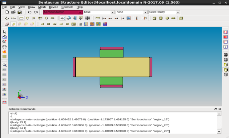
Fig 4.1 Represent the cross sectional view of Si nanowire FET

Fig 4.2 3 Dimensional structure of Si nanowire FET
V. SPECIFICATIONS
General lengths: Source and drain lengths=15nm(radius =1.5nm)
Channel length = 3nm(radius = 1.5 nm)
Gate length = 3nm(radius = 1.8nm)
Gate metal radius = 2.1nm
Total length of the nanowire is 25nm.
For nFET:
-Source/Drain Doping: Gallium Nitride (GaN)
-Channel Material: Germanium (Ge) or Silicon-Germanium (SiGe) –
High-k Dielectric: Hafnium Oxide (HfO2) -Gate Metal: Tungsten (W)
-Gate Length: Approximately 3nm -Nanowire Diameter: 3nm to 5nm
-Source/Drain Length: 20nm to 30nm -Gate Oxide Thickness: 1nm to 2nm
-Spacer Length: 5nm to 10nm
-For source and drain take constant doiping.doping uniform n.typeconc=1e19 region=1.
-For channel take analytical.doping gaussian p.type peak=1e16 loc=1.5 x char=0.5 sigma=0.1 region=2
For pFET:
-Source/Drain Doping: Gallium Phosphide (GaP) -Channel Material: Germanium (Ge) or Silicon-Germanium (SiGe)
-High-k Dielectric: Hafnium Oxide (HfO2) -Gate Metal: Cobalt (Co) or Gold (Au)
-Gate Length: Approximately 3nm -Nanowire Diameter: 3nm to 5nm
-Source/Drain Length: 20nm to 30nm
-Gate Oxide Thickness: 1nm to 2nm -Spacer Length: 5nm to 10nm
A. Equations
The equations are an exception to the prescribed specifications of this template. You will need to determine whether or not your equation should be typed using either the Times New Roman or the Symbol font (please no other font). To create multileveled equations, it may be necessary to treat the equation as a graphic and insert it into the text after your paper is styled.
Number equations consecutively. Equation numbers, within parentheses, are to position flush right, as in (1), using a right tab stop. To make your equations more compact, you may use the solidus ( / ), the exp function, or appropriate exponents. Italicize Roman symbols for quantities and variables, but not Greek symbols. Use a long dash rather than a hyphen for a minus sign. Punctuate equations with commas or periods when they are part of a sentence, as in:
a???b????? ???
Note that the equation is centered using a center tab stop. Be sure that the symbols in your equation have been defined before or immediately following the equation. Use “(1)”, not “Eq. (1)” or “equation (1)”, except at the beginning of a sentence: “Equation (1) is . . .”
B. Some Common Mistakes
- The word “data” is plural, not singular.
- The subscript for the permeability of vacuum ?0, and other common scientific constants, is zero with subscript formatting, not a lowercase letter “o”.
- In American English, commas, semicolons, periods, question and exclamation marks are located within quotation marks only when a complete thought or name is cited, such as a title or full quotation. When quotation marks are used, instead of a bold or italic typeface, to highlight a word or phrase, punctuation should appear outside of the quotation marks. A parenthetical phrase or statement at the end of a sentence is punctuated outside of the closing parenthesis (like this). (A parenthetical sentence is punctuated within the parentheses.)
- A graph within a graph is an “inset”, not an “insert”. The word alternatively is preferred to the word “alternately” (unless you really mean something that alternates).
- Do not use the word “essentially” to mean “approximately” or “effectively”.
- In your paper title, if the words “that uses” can accurately replace the word “using”, capitalize the “u”; if not, keep using lower-cased.
- Be aware of the different meanings of the homophones “affect” and “effect”, “complement” and “compliment”, “discreet” and “discrete”, “principal” and “principle”.
- Do not confuse “imply” and “infer”.
- The prefix “non” is not a word; it should be joined to the word it modifies, usually without a hyphen.
- There is no period after the “et” in the Latin abbreviation “et al.”.
- The abbreviation “i.e.” means “that is”, and the abbreviation “e.g.” means “for example”.
An excellent style manual for science writers is [7].
VI. TABLES AND FIGURES
A. Tables
Table 1 : Simulation Parameters Of Si Nanowire Fet
|
PARAMETERS |
VALUES |
|
GATE LENGTH (LG) |
50 nm |
|
SOURCE LENGTH(LS) |
50 nm |
|
DRAIN LENGTH(LD) |
50 nm |
|
DRAIN DOPING |
10^20 CM^-3 |
|
WORK FUNCTION (?) |
4.8 Ev |
|
GATE OXIDE THICKNESS |
5 nm |
|
GATE LENGTH |
18 nm |
|
SOURCE LENGHT |
10^16 CM^-3 |
|
DIELECTRIC CONSTANT |
3.9 |
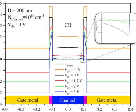
Fig : conduction band
B. Figures
The drain current variation with drain voltage for different gate-source voltage is shown in Figure 6. It can be inferred from the results that higher the gate voltage, higher is the drain current. This is because with higher gate voltage, more charge carriers are accumulated under the gate, which accomplishes high drain current.
The energy band diagram for silicon nanowire FET and Germanium nanowire FET are shown in Figures 4.1 and 4.2, respectively. It is observed from the results that for each higher applied voltage, higher are the level of conduction band in both devices, which is true for the conventional FET devices too.
The comparison of Si and Ge NW FET is given in Table 3. The mobility of InAs is very high as compared to the Si nanowire. The electron mass (m_eff) of GaN is very high as compared to the other nanowire. The characteristics of various nanowire on the basis of their parameters like diameter, length, mobility, and resistivity, permittivity, electron effective mass
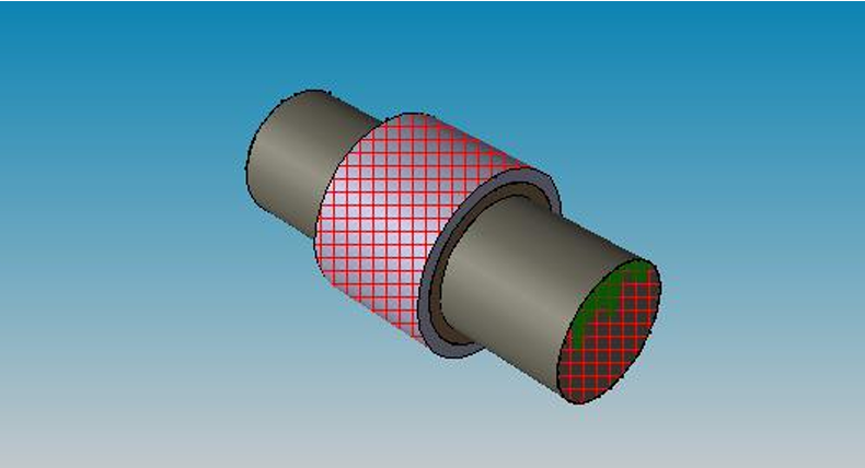
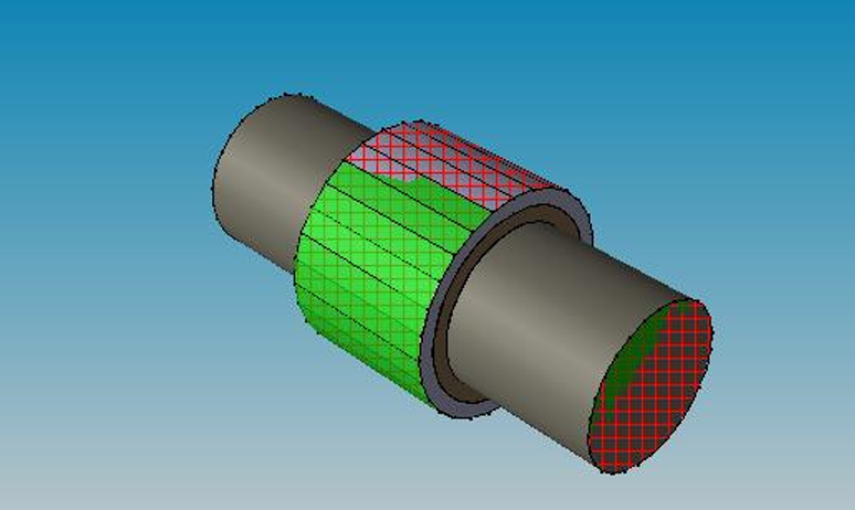
Fig : 3D design with mesh
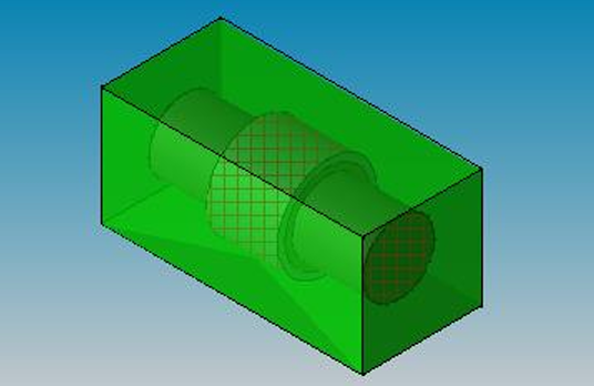
Fig : 3d design in a cubical mesh
The simulation-based comparison of proposed Si Nanowire FET and Ge Nanowire FET is performed. The SILVACO ATLAS 3D simulator was utilized to evaluate the proposed device's overall performance of ION and IOFF. The ION current of Si NW FET is 2.25 × 10^(-4) A/μm and Ge NW FET is 1.73 × 10^(-5) A/μm. The ION current of Si NW FET is very high as compared to Ge NW FET. So Ge NW FET has become more suitable for low power applications as compared to the Si NWFET. The proposed device will be suitable for low power memories design.
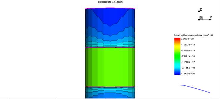
FIG : DOPING CONCENTARTION
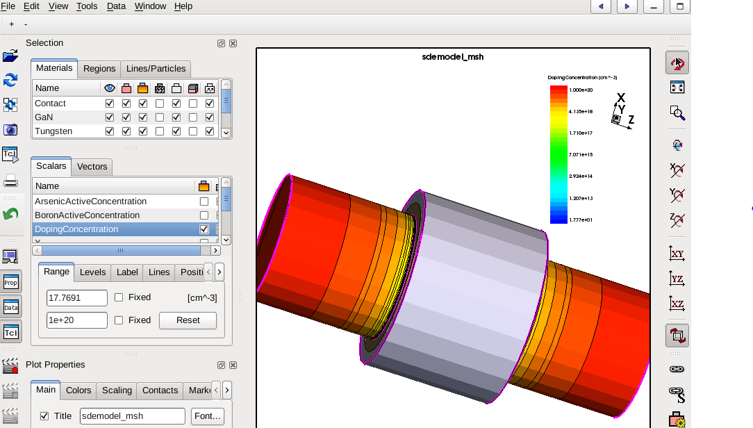
FIG : DIOPING CONCENTRATION
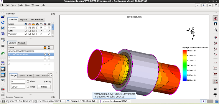
FI G: ARSENIC DOPING CONCENTRATION
C. Analysis
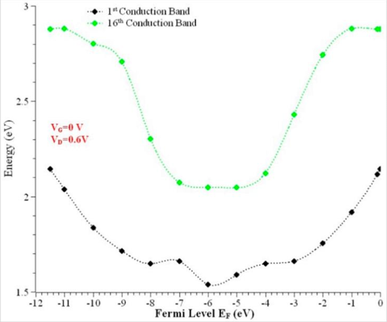
FIG : Conduction band energy using the NEGF approach
In the NFEG approach, the conduction band is formed when electrons gain enough energy to move from the valence band (where they are bound to atoms) to the conduction band (where they are free to move). This transition can occur due to thermal excitation or photon absorption.
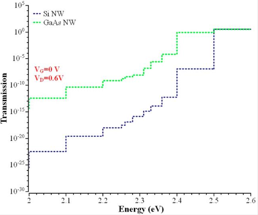
FIG : Comparisons of transmission coefficients between Si and GaAs for the 2.5 nm TrigateNanowire.
The ballistic current has been calculated by a comparison of the transmission and energy. The transmission steps depend on the channel and have high transmission regions at an energy E = 2.6 eV. The energy differences are nearly parallel; the higher transmissionobtained for both Si and GaAs nanowires are 2.8892 eV and 3.5768 at 2.6 eV. Hence, theGaAs is 1.23 times greater than Si NW. Maximum transmission can be achieved withan increase in wire dimension. Higher transmission had been achieved using differentorientations with an increase in gate bias. The transmissionspectrum has been fixed with zero gate bias (VG) and a drain voltage (VD) of 0.6 V. Whenthe gate voltage increases, higher transmission is achieved due to the lowering of thebarrier.
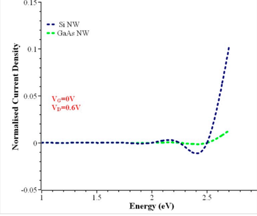
FIG : The transmissionspectrum has been fixed with zero gate bias (VG) and a drainvoltage (VD) of 0.6 V. Whenthe gate voltage increases, higher transmission isachieved due to the lowering of thebarrier.
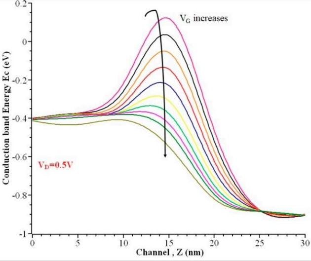
FIG : Conduction band of the GAA Nanowire
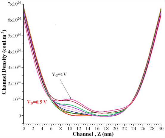
FIG : The charge density of the GAA NW along the channel
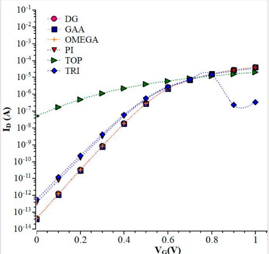
FIG : Transfer characteristics of SiNW
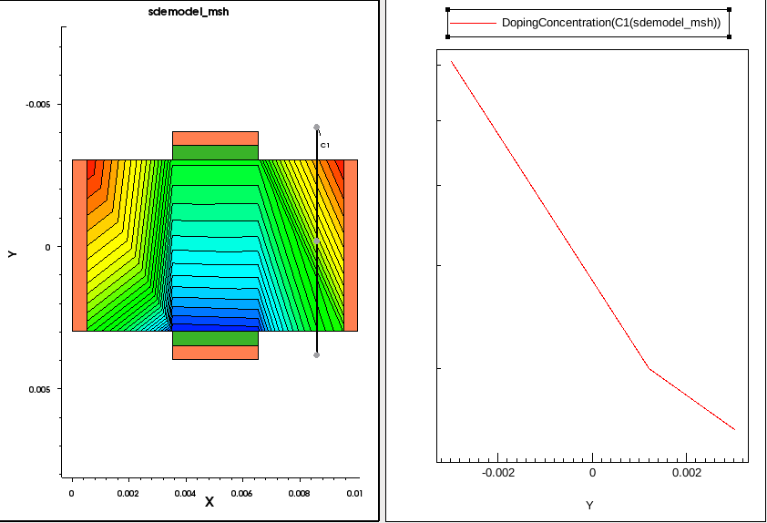
FIG : DOPING AT DRAIN BEFORE REFINEMENT
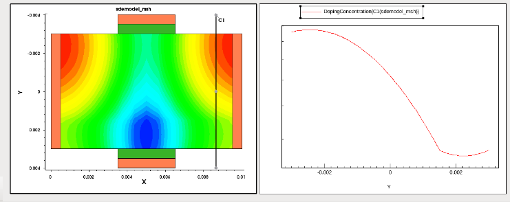
FIG : DOPING AT DRAIN AFTER REFINEMENT
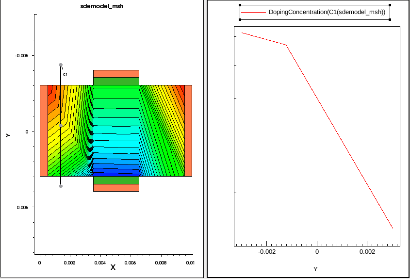
FIG : DOPING AT SOURCE BEFORE REFINEMENT
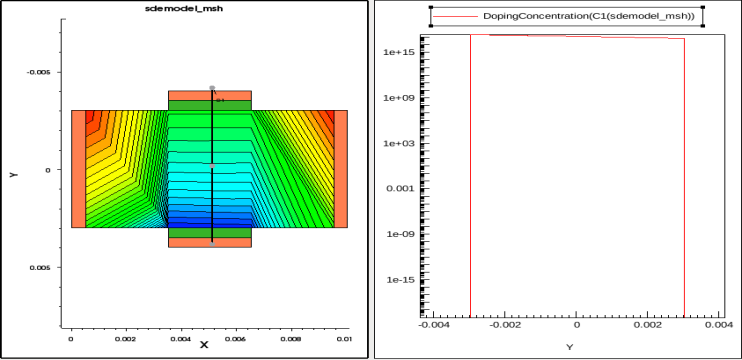
FIG : DOPING AT CHANNEL BEFORE REFINEMENT
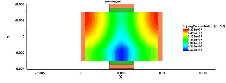
FIG : DOPING AFTER REFINEMENT
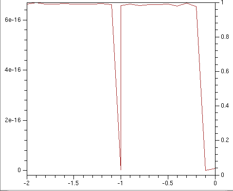
FIG : ID VS VG
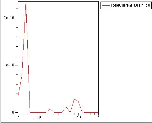
FIG : DRAIN CURRENT VS VOLTAGE
Conclusion
In this study, a simulation-based comparison of proposed Si Nanowire FET and Ge Nanowire- FET is performed. The SILVACO ATLAS 3D simulator was utilized to evaluate the proposed device\'s overall performance of ION and IOFF. The ION Current of Si NW FET is 2.25 × 10⁻⁴ A/µm and Ge NW FET is 1.73 × 10⁻⁵ A/µm. The ION current of to Si NW FET is very high as compare to Ge NW FET. So Ge NW FET has become more suitable for low power applications as compare to the Si NWFET. The proposed device will be suitable for low power memories design. GaN nanowire-based Normally-OFF transistor is simulated using TCAD-Santaurus simulator. The device performances are extracted and analyzed as a function of geometrical parameters such as nanowire diameter, drift region length, doping levels in the channel and the drift region, and surface states. The simulation results indicate that a robust Normally-OFF mode with minimum leakage current, even athigh drain voltage, is obtained when the nanowire diameter is less than 200 nm. The study also examines the impact of acceptor-type surface states on the device\'s performance and designs the device to minimize this impact. Indeed, the doping of the drift region is optimized as a function of the nanowire diameter to minimize the on-state resistance and maximize the breakdown voltage. The transverse dimensions of rectangular nanowires with similar energy levels have been examined, and the comparisons between Silicon and Gallium Arsenide NWs were investigated. The III–V compound semiconductor, such as GaAs NW, shows an attractive simulation in a few parameter results, such as transmission and electron density, compared to Silicon NW. Considering the issue of leakage current reduction, Silicon NWs are more suitable than Gallium Arsenide NWs.
References
[1] Hossain IM, Touhid K, Abu S, Alam Kutubul Nur (2021) Junctionless Gate-all around Nanowire FET with Asymmetric Spacer for Continued Scaling [2] Wang D, Wang Q, Javey A, Tu R, Dai H, Kim H, McIntyre PC, Krishnamohan T, Saraswat KC (2003) Germanium nanowire field-effect transistors with SiO2 and high-k HfO2 gate dielectrics. Appl Phys Lett 83:12 [3] Chin CY, Bo-Yi L, Meng CH (2008) Scaling Study of Nanowire and Multi-Gate MOSFETs. IEEE 978–1–4244–2186–2 [4] Sanjeet SK, Shyam K, Nishanthini L (2020) Nanowire-FET Devices for future Nanotechnology. https:// www. researchgate. net/publication/341312637 [5] Sadeghian RB, Leblebici Y, Shakouri A (2012) Simulation and design of a silicon nanowire based phase charge memory cell. Meter Res Soc 1431:20–25 [6] Chen W-H, Liu C-H, Li Q-L, Sun Q-J, Liu J, Gao X, Sun X, Wang S-D (2014) Intrinsic Ge nanowire nonvolatile memory based on a simple core–shell structure. Nanotechnology 25(7):075201. https://doi.org/10.1088/0957-4484/25/7/075201 [7] Cha HY, Wu H, Chae S, Spencer MG (2006) Gallium nitride nonvolatile memory device. J Appl Phys 100:024307 [8] Yang Y, Peng X, Kim HS, Kim T, Jeon S, Kang HK, Choi W, Song J, Doh YJ, Yu D (2015) Hot carrier trapping induced negative photoconductance in InAs nanowires toward novel nonvolatile memory. Nano Lett 15(9):5875–5882 [9] Alsheri NA, Lewis AR, Pearce-Pleydell C, Maffeis TGG (2018) Investigation of the growth parameters of hydrothermal ZnO nanowires for scale up applications. J Saudi Chem Soc 22(5):538–545 [10] Kumar P, Sharma SK, Raj B (2020) Comparative analysis of nanowire tunnel field effect transistor for biosensor applications. J Silicon 13:4067–4074 [11] Singh J, Sharma S, Raj B, Khosla M (2018) Analysis of barrier layer thickness on performance of In1-xGaxAs based Gate stack cylindrical gate nanowire MOSFET. JNO ASp 13:1473–1477 [12] Sharma SK, Raj B, Khosla M (2019) Enhanced photosensivity of highly spectrum selective cylindrical gate In1-xGaxAs nanowire MOSFET photodetector. Modern Phys Lett-B 33(12):1950144 M. Young, The Technical Writer’s Handbook. Mill Valley, CA: University Science, 1989.
Copyright
Copyright © 2025 Prateek Medida, Kareke Druvan Karthik, Ganesh D. This is an open access article distributed under the Creative Commons Attribution License, which permits unrestricted use, distribution, and reproduction in any medium, provided the original work is properly cited.

Download Paper
Paper Id : IJRASET66244
Publish Date : 2025-01-02
ISSN : 2321-9653
Publisher Name : IJRASET
DOI Link : Click Here
 Submit Paper Online

