

Ijraset Journal For Research in Applied Science and Engineering Technology
Simulation Based on High Switching Frequency H-Bridge 5-Level Multilevel Inverter Using Level Shifted In Phase Disposition (IPD) Modulation
Authors: Satish D. Patel, Parth R Mishra
DOI Link: https://doi.org/10.22214/ijraset.2025.66891
Certificate: View Certificate
Abstract
Analytical solutions of Pulse Width Modulation (PWM) strategies for multilevel Cascaded H-Bridge inverters are presented. These solutions show that the Phase Disposition (PD) PWM strategy for Cascaded H-Bridge Multilevel inverters are presented, When the carrier frequencies are adjusted to achieve the same number of total switch transitions for each inverter over one fundamental cycle. From this understanding, a method is proposed to apply the harmonically superior Phase Disposition (PD) PWM strategy for NPC inverters to Cascaded inverters, to achieve improved harmonic performance for the modulation of cascade inverters. Both theoretical and simulated results are compared and in this paper are archived result on a Simulation Based on High Swishing frequency H-Bridge Multilevel Inverter Using phase shifted Modulation using Matlab software.
Introduction
I. INTRODUCTION
While for high power applications multilevel inverters are the best available alternative, for medium or low power applications a controversy takes place. Experts on high frequency converters point out the compactness and reduced cost that can be achieved by employing high frequency switching. On the other hand, experts on low frequency converters claim that the very best efficiency and robustness belong to the topologies based on low frequency switching.
Cascaded H-bridge (CHB) multilevel inverter is one of the popular converter topologies used in high-power medium-voltage (MV) inverter. It is composed of a multiple units of single-phase H-bridge power cells. The H-bridge cells are normally connected in cascade on their ac side to achieve medium-voltage operation and low harmonic distortion. In practice, the number of power cells in a CHB inverter is mainly determined by its operating voltage and manufacturing cost. The CHB multilevel inverter requires a number of isolated dc supplies, each of which feeds an H-bridge power cell. The single-phase H-bridge power cell, which is the building block for the CHB inverter, is reviewed. Various inverter topologies are introduced. Two carrier-based PWM schemes, phase-shifted and level-shifted modulations, are analyzed and their performance is compared. A staircase modulation with selective harmonic elimination is also presented.
II. INVERTER TOPOLOGY
A. Diode-Clamped Multilevel Inverter
Fig.1 (a) shows a three-level diode-clamped inverter. The output voltage is expressed as van where n is chosen as the neutral point. The series-connecting bulk capacitors C1 and C2 can split the DC bus voltage Vdc into three levels. The switching state for different output is shown as follows:
- When the output voltage van = Vdc/2, the upper two switch S1 and S2 are closed.
- When Van = 0, the switch S2 and S1’ are closed.
- When Van = −Vdc/2, the lower two switch S1’ and S2’ are closed.
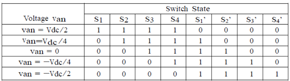
The clamping diodes D1 and D2’ play as an important role in this kind of inverter which can clamp the switch voltage to half of the DC link voltage. The output voltage van = Vdc2 is served as an example. In this case, the switch S1 and S2 should be closed. D1’ is used to balance out the voltage sharing between the two switch S1 and S2. The voltage across C1 is blocked by S1’ and the voltage across C2 is blocked by S2’ The five-level diode-clamped multilevel inverter is shown in Fig.2-1(b). The DC link voltage Vdc is evenly shared by four capacitors C1, C2, C3 and C4. The output voltage van and the corresponding switch state are shown in Table1.1..
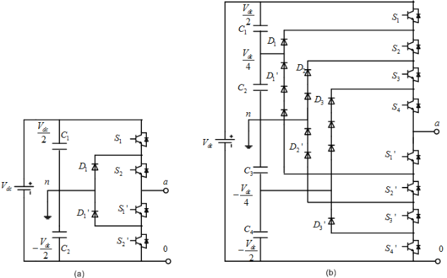
Fig. 1: Diode-clamped multilevel inverter topologies: (a) Three-level. (b) Five-level.
Table 1.1. Switching states for a 5 level Diode-Clamped Inverter.
B. Capacitor-Clamped Multilevel Inverter
In Fig.2, the topologies of the three-level and five-level capacitor-clamped multilevel inverter are presented. They have similar structure as the diode-clamped multilevel inverter. The capacitors are used in the topology instead of diodes.
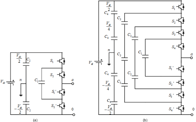
Fig. 2: Diode-clamped multilevel inverter topologies: (a) Three-level.(b) Five-level.
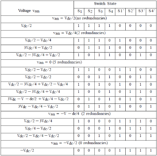
The three-level capacitor-clamped multilevel inverter is shown in Fig.2-2(a). One advantage of this kind of topology is that it can provide some redundancies for a certain output voltage. Taking the three-level Capacitor-Clamped Inverter as an example, for Van = 0, either pair (S1, S1’) or (S2, S2’) needs to be turned on. The number of redundancies will increase as the output voltage level increases. The switch state and its corresponding output voltage for five-level capacitor-clamped Inverters are shown in Table 2.2. With these redundancies, the capacitor voltages can be easily balanced with some control strategies and modulation methods since it is possible to choose which capacitor is to be charging and which one is to be discharging
C. Cascaded H-bridge multilevel inverter.
The Cascaded H-Bridge (CHB) multilevel inverter is based on the series connection of single phase H-bridge inverters with separate DC sources. The topology is shown in Fig.2-3. The output phase voltage is synthesized by the addition of the voltages that are generated by different modules. If the separate DC sources have the same voltage level (Vdc), the resulting phase voltage will be able to range from −nVdc to nVdc which would have (2n + 1) levels. And n is the number of the total modules or the number of separate DC sources. As the number of DC sources increases, there would be more levels in the output voltage. So the output voltage waveform will be nearly sinusoidal, even without filtering.
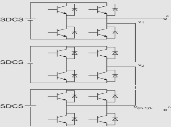
Fig. 3: CHB multilevel inverter topology.
III. MULTILEVEL MODULATIONS
When it comes to multilevel inverter modulation there are several ways to classify modulation techniques. Here, the way shown in is adopted and graphically presented in Fig.4. Multilevel modulations are meant to produce an average output voltage proportional to the reference given by some external algorithm, while multilevel controls are meant to apply an output voltage calculated by them, like Multilevel Direct Torque Control (MDTC).
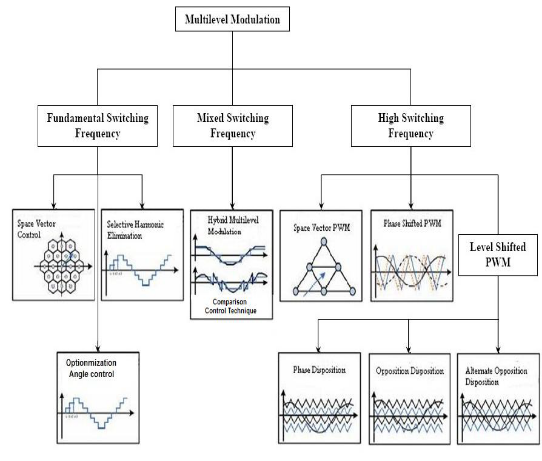
Fig.4: Classification tree for multilevel modulations.
A. Level Shifted PWM (LSPWM)
1) In Phase Disposition(IPD)
Level Shifted PWMs use more carriers, with the same amplitude and frequency, but translated in level as pictures in Fig, 5, show for a 5-level inverter. The number of carriers needed to generate the driving signals for an n-level converter is the same as PSPWM that is n-1.There are three major kinds of LSPWMs depending on how the carriers are disposed. The most evident method, depicted in Fig.5, is called In Phase Disposition (IPD).
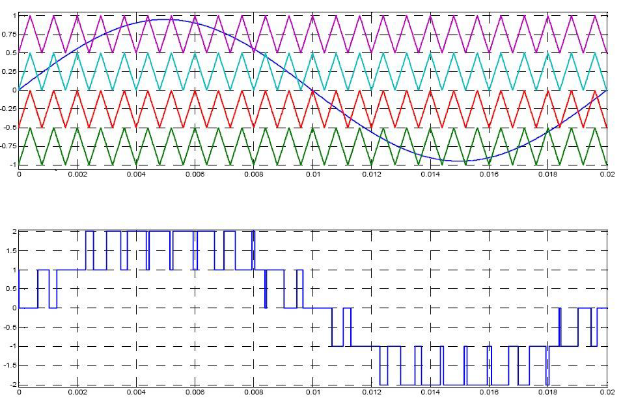
Fig. 5: LSPWM carriers and reference for a 5-level converter, In Phase Disposition (IPD)
The interval of possible voltage reference values is subdivided into one zone for each carrier which modulates the output only when the reference belongs to its zone. When the reference does not belong to a zone, associated carrier comparison output is fixed to high or low level: it is high when the reference is above the carrier; vice versa it is low when the reference is under the carrier. The comparison output, obtained in this way, and its negation can directly drive a couple of switches in diode-clamped. The sum of all the comparison outputs, shown in Fig.5, is a signal proportional to the instantaneous required output level.
2) Phase opposite Disposition (POD)
The Phase Opposition Disposition (POD) uses the same translation of carriers as IPD, but the carriers associated to negative levels are in opposition of phase as depicted in Fig.3-10. Fig.3-10 shows the signal obtained as sum of comparison output signals and it is proportional to the level required.
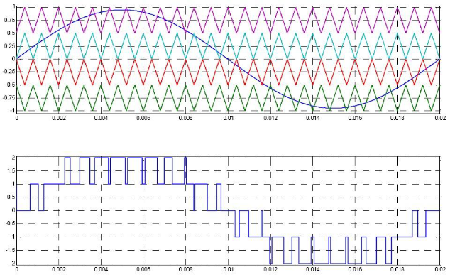
Fig.6: LSPWM carriers and reference for a 5-level converter, Phase Opposition Disposition (POD)
3) Alternative Phase Opposition Disposition (APOD),
The Alternative Phase Opposition Disposition (APOD), depicted in Fig.7, has the carriers alternatively in phase or in opposition. Fig. 7 shows the output required by this kind of modulation. As it can be seen comparing Fig.5, 6 and 7, the difference among these three LSPWMs is related to the symmetry of the output they produce. Indeed, POD and APOD have odd symmetry, while IPD positive half-wave can be mirrored and translated to coincide with the negative one. Each switch commutates at the carrier frequency only.
When the reference belong to the zone related. Otherwise the switch is hold, but the converter is still commutating. This means that the switching frequency of the converter is equal to the carrier frequency ( fcar ), but the average switching frequency of the single switch ( fsw) is lower and, for a n-level converter, it is given by (1)
------------------(1)\
Anyway, the carrier frequency has to be suited for the characteristics of the chosen switchs, so in LSPWM do not really allow to increase the output frequency as PSPWM does.
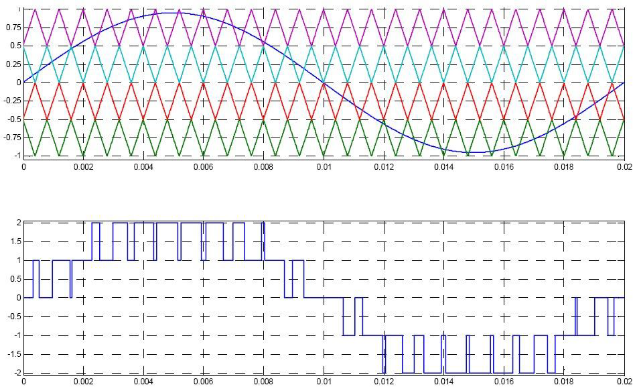
Fig. 7: Level Shifted PWM carriers and reference for a 5-level converter, Alternative Phase Opposition Disposition (APOD).
IV. SIMULATION RESULT ON A 5- LEVEL IN SHIFTED DISPOSITION(IPD) MLI
The Matlab Simulink Model for single phase 5-level MLI using Level Shifted PWM Technique in phase disposition is shown in Fig.8. however few changes of no. of carriers and phase change of triangular carrier waves are required according to modulation techniques. LSPWM carriers and reference for a 5-level converter, and variance gate pulse on Mosfet In Phase Disposition (IPD) MLI and LSPWM carriers and reference for a 5-level converter, and variance gate pulse on Mosfet In Phase Disposition (IPD) MLI and Output voltage and FFT of 5-level Converter using IPD, modulation techniques is shown in fig.9, 10 and 11 respectively.
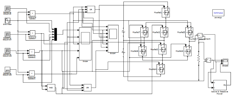
Fig.8.Simlink using 5 level in shifted disposition MLI.
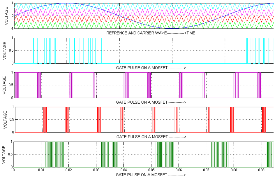
Fig. 9: LSPWM carriers and reference for a 5-level converter, and variance gate pulse on Mosfet In Phase Disposition (IPD) MLI

Fig. 10: LSPWM carriers and reference for a 5-level converter, and variance gate pulse on Mosfet In Phase Disposition (IPD) MLI
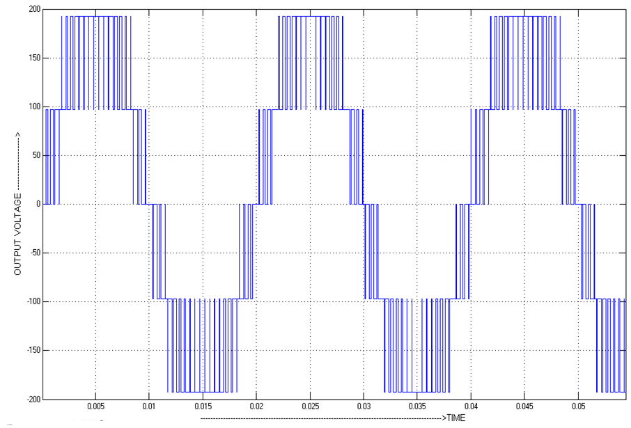
Fig. 10: Output voltage for a 5-level In Phase Disposition (IPD) MLI
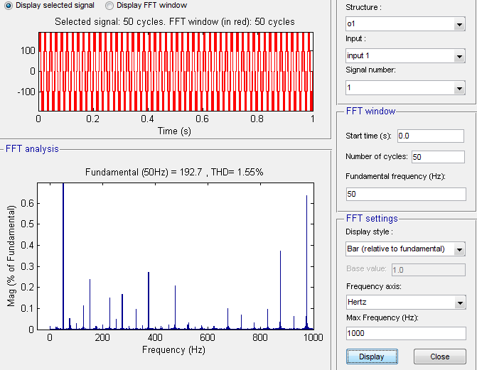
Fig. 11: THD on a Output voltage for a 5-level In Phase Disposition (IPD) MLI
Conclusion
In this paper Simulation result achieved High Switching Frequency H-Bridge Multilevel Inverter Using Level Shifted In Phase Disposition (IPD) Modulation using MATLAB Software, and desired output voltage THD is 1.55%, in this LSPWM is good opportunity for the realization of the single-phase inverter control and reduced harmonic distortion.
References
[1] HIGH-POWER CONVERTERS AND AC DRIVES IEEE Press 445 Hoes Lane Piscataway, NJ 08854 IEEE Press Editorial Board Mohamed E. El-Hawary, Editor in Chief. [2] B. P. McGrath and D.G. Holmes “A Comparison of Multicarrier PWM Strategies for Cascaded and Neutral Point Clamped Multilevel Inverters” Department of Electrical and Computer Systems Engineering, Monash University Wellington Road, Clayton, 3 168, AUSTRALIA. [3] Leon M. Tolbert, Fang Z. Peng ,”Multilevel PWM Methods at Low Modulation Indices” 0-7803-5160-6/99/$10.00 0 1999 IEEE [4] Leon M. Tolbert, Thomas G. Habetler Novel Multilevel Inverter Carrier-Based PWM Methods 0-7803-4943-1/98/$10.00 0 1998 IEEE [5] Brendan Peter McGrath and Donald Grahame Holmes “Sinusoidal PWM of Multilevel Inverters in the Overmodulation Region “0- 7803-7262-X/02/$10.00 0 2002 IEEE. [6] Power electronics devices and application by Mahmud h. Rashid.
Copyright
Copyright © 2025 Satish D. Patel, Parth R Mishra. This is an open access article distributed under the Creative Commons Attribution License, which permits unrestricted use, distribution, and reproduction in any medium, provided the original work is properly cited.

Download Paper
Paper Id : IJRASET66891
Publish Date : 2025-02-10
ISSN : 2321-9653
Publisher Name : IJRASET
DOI Link : Click Here
 Submit Paper Online