

Ijraset Journal For Research in Applied Science and Engineering Technology
Implementation of 8-Bit Asynchronous SAR ADC
Authors: P. Durga Prasanna, D. Srinivasulu Reddy
DOI Link: https://doi.org/10.22214/ijraset.2025.67010
Certificate: View Certificate
Abstract
This study analyses the design of SAR ADC that is suitable for implementing in low power applications. The designed SAR ADC minimizes the complexities associated with its design using higher frequencies by avoiding the usage of oversampled clock. A Bootstrap circuit is designed for a sampling and holding which improves increased linearity. Another aspect of the low power is designing a comparator such that it does not require a pre-amplifier. Successive Approximation register (SAR) ADC is implemented using a charge redistribution DAC. The SAR logic block generates the digital code thus reducing power consumption in the circuits. Hence, an 8-bit SAR ADC that exhibits a maximum sampling frequency of 20MHz using 250 nm CMOS technology is designed in S-SDIT Tanner and its working is verified through circuit level simulations.
Introduction
I. INTRODUCTION
Analog to digital converter can be understood in various ways, such as counter type ADC, Flash ADC, Dual slope ADC. Apart of these ADCs, only SAR ADC is the one widely used for précised and accurate, medium speed conversion of Analog signal. It uses a feedback scheme to approximate each analog sampled signal to digital equivalent value. It contains Sample and hold circuit, Digital to Analog Converter (DAC), SAR and a voltage comparator. The accuracy of ADC is mainly depends on the precision of DAC matching component and comparator’s ability to resolve small change difference between input and output of DAC. The speed of ADC indirectly depends on settling time of both DAC and comparators. Speed of SAR ADC depends on the size of ADC i.e. number of bits required to represent the output. Analog-to-digital converters (ADCs) that function at low power levels have been widely used for various applications, such as biomedical instrumentation applications and wireless sensor networks, for economizing energy consumption. For low-power and low-speed (below several tens of MS/s) system applications, successive approximation register analog-to-digital converter (SAR ADC) has been a popular candidate among the various types of ADCs because it has many advantages such as moderate resolution and speed, no static power consumption, and a simpler structure. Moreover, with the feature sizes of CMOS devices scaled down, SAR ADCs can be operated at higher conversion rate and lower power consumption. In the recent years, the efficiency and capability of ADCs have raised gradually in achieving reduced power consumption leading to medium speed and high resolution. In general, ADCs are divided into four types namely, Delta, SAR, Pipeline and Flash as shown in the Fig 1, Delta type ADCs comply with applications that require increased resolution and operates at lower bandwidth. SAR ADCs are successful for applications that require standard resolution and speed of sampling varying from small to moderate levels. Pipeline ADCs are used in applications that require faster speed of sampling and increased resolution. Flash ADCs generates enormous high speed sampling with lower resolution. SAR ADCs use the algorithms like binary search with a closed-loop system which generates a data sample following a chain of continuous iterations producing a comparatively minimal rate of sampling than that of delta, pipeline and flash ADCs. Since low power is a major factor in this project, the use of SAR ADC architecture does not need more comparators or opamps to be used. By this, it reduces the power to a great extent.
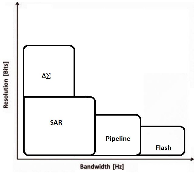
Fig 1 Different types of ADCs
In summary, SAR ADCs reduces the schematic complexity and power which is a major concern when used in low power battery operated biomedical applications. It only requires medium speed and medium resolution with reduced power consumption. Several important methods and design practices for improving its efficiency have been recommended endlessly.
II. PREVIOUS WORKS
Yan Zheng et al., proposed a 13-bit 100MS/s SAR ADC. In this paper [12], a three stage comparator based inverter is implemented to enhance the speed. Also to keep the comparator noise low as it affects the speed. In addition to it, an improved asynchronous logic circuit with feedback is implemented to reduce the leakage current of the transistor. The proposed architecture has simple configuration and high digital nature because of which it is energy efficient. This methodology is fabricated in SMIC 14nm CMOS FinFET consuming 2.34mW power. The limitation in this paper is that the trade-off between noise and power in comparator is not linear.
Sanjeev et al., proposed a single channel band pass SAR ADC architecture which can be ported into advance technologies to improve speed and to reduce power, because of its high digital nature. The proposed architecture in this [13] work diminishes the drawbacks and also there are 5x improvements in energy efficiency that is associated with existing Band pass SAR ADC architecture. The off-chip implementation of Maximum Likelihood Estimation will allow us to check different noise transfer function. It also improves the signal-to-noise ratio. The prototype of the proposed ADC is fabricated in 65nm CMOS technology consuming 17uW power and BP-FoM of 29fJ/step for 100 KHz. The temperature limit has to be 60°C to avoid damaging of plastic components on the test-board.
The work proposed by Guanhua Wang et al., presents a 1-GS/s 3.2-mW 8-bit SAR ADC implemented in 28-nm CMOS technology uses background-calibrated coarse and fine comparators to reduce the power consumption. The proposed SAR ADC architecture [14] is shown below in Fig 2.1. The comparator approach here has a redundant DAC to control both the DAC settling errors and comparator errors. In this [14] design, the 9th bit is not chosen to perform the offset calibration because the decision of the 9th bit is very close to the DAC reset cycle and would affect the calibration accuracy and instead the 7th bit and 8th bit is used. The total offset calibration area is 25% approximately of the total ADC area with a total offset calibration power consumption of 0.34 mW.
By using the proposed reference comparator calibration scheme, the calibration time is removed from the SAR timing budget completely. The prototype ADC achieves the SNDR of 43.6 dB near Nyquist frequency with FOM 25.87 fJ/conversion-step. Naveen et al. discusses a twelve bit successive ADC utilized for increased battery- life applications. A capacitor split technique is used to enhance the complete speed of the circuit. Additionally in order to attain high sampling linear operation, the technique of bootstrapped switching is used. The method used in [15] paper will prevail over area and large current consumption that is caused in 0.180um, 0.09um and 0.065um complementary metal oxide semiconductor technologies. Besides this, the method was executed in 0.045um CMOS technology. The proposed circuit configuration operated at 0.004667nanowatts power and 2330.6μm² silicon die. Additionally to implement this configuration, it requires more number of circuit blocks, which in turn drastically upsurges the complexity of ADC.
III. PROPOSED METHOD
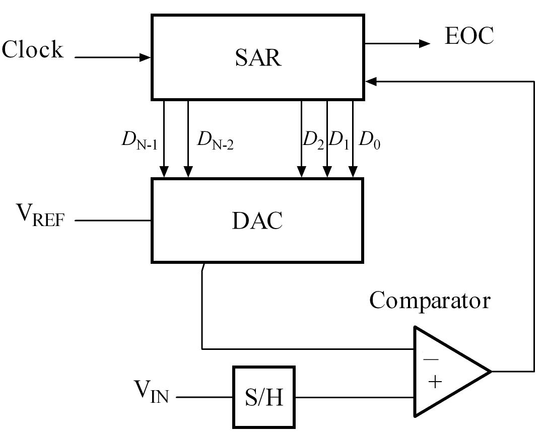
Fig. 2 Block diagram of SAR ADC
SAR ADC contains a sample-hold circuit, a comparator circuit ,a SAR logic circuit and a digital to analog converter circuit as as shown in Fig 2.The sample-hold circuit takes the voltage of a constantly changing analog signal Vin and carries its value at a steady state for a defined short interval of time. The comparator takes both the sample-hold schematic voltage output VS/H and the voltage output generated by the DAC VDAC, for comparison. It performs N number of binary bit comparison iterations until generating a digital value with respect to outcome of the comparison. SAR ADC uses a binary search methodology, inorder to transform analog input waveform to digital output waveform.
The architecture "Asynchronous” denotes that all the blocks in the Fig 2, do not function with an identical constant clock signal. Every block in the architecture generates a signal such that the following block depends on the signal to modify its current state. The clock that is used externally activates the Clock block to start the transition operation. The Clock block genarates five clock signals. The "Sclka" and "Sclkb" are clock pulse signals that are used in Bootstrap Circuit for sampling. The comparator is controlled by using the "Sarclkb" clock signal and the SAR Logic uses the "Sarclk" and "Sclk" signals to modify the voltage of the DAC block. The Bootstrap block samples the input signal and begins the transition operation, where the SAR logic employs the code in the DAC when the "Sarclk" signal becomes high.
IV. RESULTS AND DISCUSSIONS
The implemented Bootstrap circuit in S-Edit is shown in Fig. 3 below.
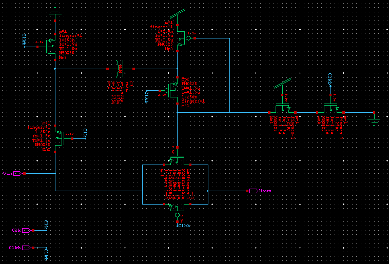
Fig 3 Implemented Bootstrap Block
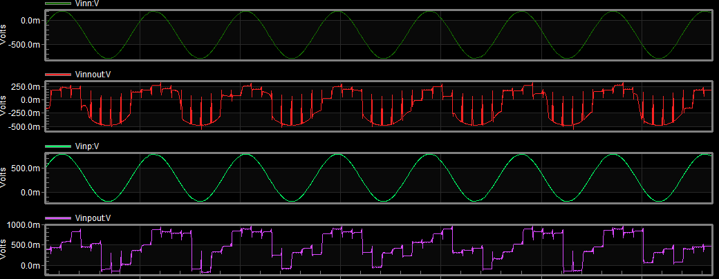 Fig 4: Output waveform of the Bootstrap Block
When the clk is 0,the switches Mn2, Mp2, Mn3, Mp3 are in the holding state which are utilized to charge the offset capacitor c3 and when the clk is 1, it maintain the voltage across the gate and the source of the Mn5.when the voltage across the gate and the source is high, this confirms that the main switch Mn5 is fully in ON state and it is higher than the set point with the voltage of Mn5 varying. In the Sampling time, the gate terminals of Mn5 and Mp1 are binded together as the voltage of Mn5 and Mp3 are higher than that of the supply voltage. When the Mp1 is in OFF state, its gate is binded to the circuit that is having highest voltage. Also the switches Mp2 and Mp3 are linked to the positive terminal of the offset capacitor c3 which has the highest voltage. At the time of holding,Mn4 secures the main switch Mn5 to shut down by causing it to go to OFF state by connecting it to the lowest voltage. When Mn4 is in OFF state, in order to avoid high voltage across the gate and the drain .If the offset capacitor value of the c3 is high, during the sampling stage, it strongly maintains a constant voltage. Since both Mn5 and Mp1 switches are connected in parallel the there is no need for cross-connections as they both function as different clocks. From the waveforms of the bootstrap block in Fig. 4, it can be understood that when the clock goes high that is ‘1’, the outputs “Vinpout” and “Vinnout” tracks the input and when it goes low that is ‘0’, it holds the values. The implemented SAR Logic Block circuit is shown in the Fig. 5 below.
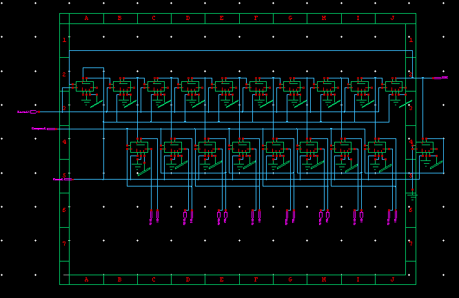
Fig 5: Implemented SAR Logic Block
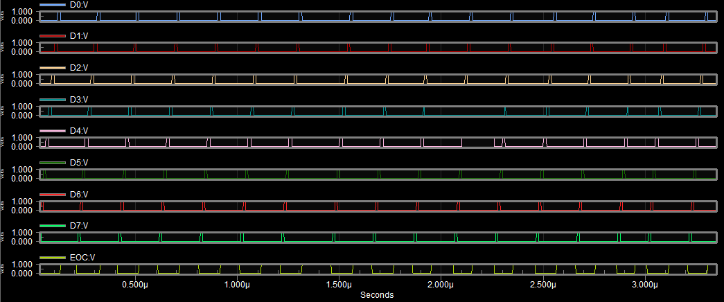 Fig 6: Output waveforms of the SAR Logic Block
Conclusion
An asynchronous SAR ADC is designed with 8-bit resolution and supply voltage of 1V with a frequency of 20MHz using S-Edit Tanner Tool using 270nm technology. The architecture utilizes a clock block which manages the transition operation by producing the necessary clock signals for the entire system. In order to minimize the distortion and enhance the speed, the differential input signal is sampled by the Bootstrap Block. The DAC block uses charge-redistribution technique with binary weighted capacitance values in order for the comparator to compare the input values without absorbing the power when there is no circuit activity. A strong arm regenerative latch based comparator block attains reduced delay, minimizing the wastage of power, and low offset. By utilizing the true-single phase clock type flip-flops, the SAR logic block minimizes the power dissipation thereby producing the digital code. Thus the achieved total power consumption and delay are found to be promising by utilizing the improved bootstrapped switching and strongarm latch techniques.
References
[1] T.O. Anderson. Optimum control logic for successive approximation analog-todigital converters. Communications Systems Research Section, JPL Technical Report 32-1526, Vol XIII. [2] Shuo-Wei Mike Chen, Robert W. Brodersen. A 6b 600MS/s 5.3mW asynchronous ADC in 0.13µm CMOS. IEEE international solid-state circuits conference, 1-4244-0079-1, 2006. [3] Pieter J. A. Harpe, Cui Zhou, Yu Bi, Nick P. van der Meijs, Xiaoyan Wang, Kathleen Philips, Guido Dolmans, Harmke de Groot. A 26 µW 8 bit 10 MS/s asynchronous SAR ADC for low energy radios. IEEE journal solid-state circuits, Vol. 46, No 7, 2011. [4] Tsuguo Kobayashi, Kazutaka Nogami, Tsukasa Shirotori, Yukihiro Fujimoto. A current-controlled latch sense amplifier and a static power-saving input buffer for low-power architecture. IEEE Journal of solid-state circuits, Vol. 28, No 4. 1993 [5] J. Fredenburg and M. P. Flynn, \"ADC trends and impact on SAR ADC architecture and analysis,\" 2015 IEEE Custom Integrated Circuits Conference (CICC), San Jose, CA, 2015, pp. 1-8. [6] S. Zhang, K. Huang and H. Shen, \"A Robust 8-Bit Non-Volatile Computing-in-Memory Core for Low-Power Parallel MAC Operations,\" IEEE Transactions on Circuits and Systems I: Regular Papers, 2020. [7] M. Daliri, Mohammad Maymandi-Nejad, K. Mafinezhad, \"Distortion analysis of bootstrap switch using Volterra series\",January 2010, 3(6):359 - 364, DOI:10.1049/iet-cds.2008.0354 [8] Michael D. Scott,Bernhard E. Boser,and Kristofer S. J. Pister,\"An Ultralow-Energy ADC for Smart Dust\",IEEE JOURNAL OF SOLID-STATE CIRCUITS, VOL. 38, NO. 7, Page(s): 1123 - 1129,JULY 2003. [9] J. Yang, T. L. Naing and R. W. Brodersen, \"A 1 GS/s 6 Bit 6.7 mW Successive Approximation ADC Using Asynchronous Processing,\" in IEEE Journal of Solid-State Circuits, vol. 45, no. 8, pp. 1469-1478, Aug. 2010, doi: 10.1109/JSSC.2010.2048139 [10] Hedayati, Raheleh. \"A study of Successive Approximation Registers and implementation of an ultra-low power 10-bit SAR ADC in 65nm CMOS technology.\" (2011). [11] C. Liu, S. Chang, G. Huang and Y. Lin, \"A 10-bit 50-MS/s SAR ADC With a Monotonic Capacitor Switching Procedure,\" in IEEE Journal of Solid-State Circuits, vol. 45, no. 4, pp. 731-740, April 2010, doi: 10.1109/JSSC.2010.2042254. [12] Yan Zheng;Fan Ye; Junyan Ren-“ A 13 bit 100 MS/s SAR ADC With 74.57 dB SNDR in 14-nm CMOS FinFET”, published by IEEE 2020 [13] Sreenivasulu Polineni; M. S. Bhat; S. Rekha- “A switched capacitor-based SAR ADC employing a passive reference charge sharing and charge accumulation technique”, published by Birkhauser 2020 [14] Sanjeev Tannirkulam Chandrasekarum; Gaurav Kapoor; Arindam Sanyal- “8fJ/Step bandpass ADC with digitally assisted NFT re-configuration”, published by IEEE 2020 [15] B. Satish; Prabhu G Benakop- “Design and implementation of energy efficient SAR analog to digital converter”, published by Blue Eyes Intelligence Engineering & Sciences Publication 2019 [16] Guanhua Wang; Kexu Sun; Qing Zhang; Salam Elahmadi; Ping Gui “A 43.6-dB SNDR 1-GS/s 3.2-mW SAR ADC with background-calibrated fine and coarse comparators in 28-nm CMOS”, published by IEEE 2019 [17] Naveen I .G; Savita sonoli-“ Design of 12-Bit SAR ADC using split capacitor based DAC architecture at 45nm CMOS technology”, published by Blue Eyes Intelligence Engineering & Sciences Publication 2019 [18] Haoyu Zhuang; Wenjuan Guo; Jiaxin Liu; He Tang; Zhangming Zhu; Long Chen; Nan Sun- “A Second-Order Noise-Shaping SAR ADC with Passive Integrator and tri-level voting”, published by IEEE 2019 [19] Andrea Di Salvo- “Design of a 12-bit SAR ADC with digital self-calibration for radiation detectors front-ends”, published by IEEE 2019 [20] Jun-Eun Park; Young-Ha Hwang; Deog-Kyoon Jeong- “A 0.5-V Fully Synthesizable SAR ADC for On-Chip Distributed Waveform Monitors”, published by IEEE 2019 [21] Jian Luo; Yang Liu- “A Low Voltage and Low Power 10-bit Non-Binary 2b/Cycle Time and Voltage Based SAR ADC”, published by IEEE 2019 [22] Mojtaba Bagheri; Filippo Schembari; Naser Pourmousavian; Hashem Zare-Hoseini; David Hasko; Robert Bogdan Staszewski- “A Mismatch Calibration Technique for SAR ADCs Based on Deterministic Self-Calibration and Stochastic Quantization”, published by IEEE 2019 [23] Aleksandr Gusev; Dmitry Osipov; Steffen Paul- “Multi-step capacitor switching scheme for low-power SAR ADC”, published by ITEM 2019 [24] Akshay Jayaraj; Sanjeev Tannirkulam Chandrasekaran; Archana Ganesh; Imon Banerjee; Arindam Sanyal- “Maximum Likelihood Estimation Based SAR ADC”, published by IEEE 2018
Copyright
Copyright © 2025 P. Durga Prasanna, D. Srinivasulu Reddy. This is an open access article distributed under the Creative Commons Attribution License, which permits unrestricted use, distribution, and reproduction in any medium, provided the original work is properly cited.

Download Paper
Paper Id : IJRASET67010
Publish Date : 2025-02-18
ISSN : 2321-9653
Publisher Name : IJRASET
DOI Link : Click Here
 Submit Paper Online