Ijraset Journal For Research in Applied Science and Engineering Technology
- Home / Ijraset
- On This Page
- Abstract
- Introduction
- Conclusion
- References
- Copyright
Implementation of Digital Filter Using Verilog HDL
Authors: V. Vittal Reddy , Udathu Jaya Madhuri , Vutukuri Sailaja , Zubera Farheen Khatun, Velpula Jagadish Kumar
DOI Link: https://doi.org/10.22214/ijraset.2024.60579
Certificate: View Certificate
Abstract
In the context of Very Large Scale Integration technology, where addition is essential, digital filters are essential elements. The performance of the Finite Impulse Response Filter is highly dependent on the speed of its multiplier unit, making it stand out among the others. In order to improve the effectiveness of the FIR filter, we suggest using a Wallace tree multiplier. This novel method offers improvements over conventional multipliers, with a decrease in latency being one of the main advantages. Significant improvements in latency are obtained by using Xilinx tools and implementing this filter design in Verilog HDL. The Wallace tree multiplier is perfect for FIR filter construction in low-voltage and low-power VLSI applications since it has benefits like higher operating frequency and reduced power consumption. This development might improve the effectiveness and performance of digital filters, especially in settings with limited resources, opening the way for more robust VLSI systems.
Introduction
I. INTRODUCTION
In the realm of Very Large Scale Integration (VLSI) technology, digital filters stand as indispensable components, providing essential signal processing capabilities. Among these, the Finite Impulse Response (FIR) Filter holds particular significance, owing to its widespread use and critical role in numerous applications. Central to the performance of FIR filters is the speed of their multiplier units, which directly impacts their effectiveness in processing digital signals with minimal delay. Enhancing the efficiency of FIR filters has thus become a key focus within the VLSI community, prompting innovative approaches to address latency and power consumption concerns. The Wallace tree multiplier presents itself as a potential remedy for the need for enhanced FIR filter performance. Significant benefits over conventional designs are provided by this innovative multiplier architecture, particularly in terms of power efficiency and latency reduction. Multiplication operations may be performed more quickly by taking use of the Wallace tree structure's intrinsic parallelism, which helps to reduce the bottleneck that multiplier units in FIR filters are known for. With minimal latency and power conservation being critical factors in VLSI applications, this breakthrough marks a major advancement in digital filter design optimisation.
The Wallace tree multiplier's practical benefits may be realised through its implementation, which is made easier by Xilinx tools and Verilog Hardware Description Language (HDL). Engineers may easily create effective FIR filter designs with Verilog HDL's strong modelling and simulation framework for complicated digital systems. Additionally, the implementation workflow is streamlined by interaction with Xilinx tools, which provide thorough assistance for operations related to synthesis, place-and-route, and verification. Engineers may use the Wallace tree multiplier to significantly increase the performance of FIR filters, especially in low-voltage and low-power VLSI applications, by using this well-organized development environment.
A major development in VLSI technology, the Wallace tree multiplier's usage in FIR filter design offers improved performance and efficiency for a variety of applications. This novel technique tackles important issues facing digital filter implementations in contemporary VLSI systems by lowering latency and power consumption while retaining high operating frequencies. Engineers may achieve noticeable gains in FIR filter designs by utilising the combination of Verilog HDL, Xilinx tools, and Wallace tree multiplier architecture. This will open the door for more resilient and energy-efficient VLSI systems in the digital era.
A. Objectives
- The primary goal of the work is to use a Wallace tree multiplier architecture to create a Finite Impulse Response filter. The purpose of this architecture is to increase the FIR filter's multiplication operations' speed in order to lower latency and boost overall performance.
- Achieving low power consumption in the FIR filter design is a key focus of the research. The goal is to save energy without sacrificing performance by using the Wallace tree multiplier, which has intrinsic power efficiency advantages over conventional multiplier designs.
- Because it can perform multiplication operations in parallel, the Wallace tree multiplier is used to compute filter outputs more quickly. Speed is emphasised here because real-time signal processing applications require quick responses.
- The endeavour recognises that when designing FIR filters, space and hardware complexity must be traded off. Compared to conventional multiplier implementations, the Wallace tree multiplier may demand more hardware resources despite its advantages in speed and power efficiency.
- A comparison study will be carried out in order to assess the effectiveness and performance of the suggested system. In this investigation, the Wallace tree multiplier-implemented FIR filter's performance metrics such as latency, power consumption, and resource utilization will be compared to those of a conventional multiplier-based FIR filter.
II. RELATED WORK
Using FPGA platforms, A. R. Kumar, B. Sriraj, K. H. L. P. Prasad, and P. R. Rajasri offer a new method for building a systolic finite impulse response (FIR) filter[1] The authors' main goal is to achieve effective filtering operations in FPGA settings by utilizing the single-channel approach. They seek to improve FIR filtering jobs' performance and throughput by utilizing the systolic architectures' inherent parallelism and pipelining capabilities. The design factors, implementation techniques, and experimental findings from their FPGA-based FIR filter prototype are covered in this study. The authors show the efficacy and applicability of their suggested technique for practical applications in cloud computing, data science, and engineering via thorough examination and analysis. In this article, N. Chabini and R. Beguenane investigate the design and implementation of digital Finite Impulse Response (FIR) filters based on FPGAs that are optimized for situations involving large data input and small coefficients. They also discuss the difficulties these scenarios present and suggest FPGA-specific solutions[3]. The authors explore the complexities of fine-tuning FIR filter designs to effectively handle tiny coefficient values while preserving reliable performance with massive input data streams. Their study provides important insights into the design of FIR filters in particular, which is relevant to the development of FPGA-based digital signal processing systems. The study's conclusions and methodology, which highlight developments in FPGA-based digital signal processing techniques, are applicable to a wide range of computer and communication systems where FIR filtering is used.
In the field of Very Large Scale Integration (VLSI), N. Udaya Kumar, U. Subbalakshmi, B. Surya Priya, and K. Bala Sindhuri explore the complexities of implementing Finite Impulse Response (FIR) filters using different addition and multiplication techniques[5]. They provide a thorough examination of the various approaches used in the VLSI domain to efficiently realize FIR filters. The authors want to find the best methods by examining several addition and multiplication strategies that strike a balance between efficiency, area use, and power usage. Their work sheds light on the trade-offs involved in selecting particular arithmetic operations in VLSI applications, which is helpful in understanding the design and implementation of FIR filters.
The practical aspects of implementing Finite Impulse Response (FIR) filters using Field-Programmable Gate Arrays (FPGAs) and Verilog Hardware Description Language (HDL) are explored by L. Y. Akshitha V. Ramesh, Apeksha Ravi Kumar, and Amulya S. Iyengar[7]. They offer insights into the process of designing and realising FIR filters on FPGA platforms, utilising the capabilities of FPGA for hardware implementation and Verilog HDL for digital circuit modelling. In order to accomplish effective and high-performance filtering operations, the authors examine numerous design considerations, approaches, and optimisation strategies used in the construction of FIR filters. Through the integration of theoretical concepts with real-world implementation specifics, the study provides insightful advice for academics and engineers working on digital signal processing and FPGA-based system design.
The creation of Finite Impulse Response (FIR) filters implemented on Field-Programmable Gate Arrays (FPGAs) is the subject of study by S. Chao, Q. Hui, S. Tong, M. Junzhi, Z. Yongjie, and D. Jianjun. With an emphasis on performance, resource efficiency, and power economy, the authors explore the complexities of creating FIR filters especially for FPGA-based implementations[9]. The goal of the authors' use of FPGA technology is to provide effective and real-time signal processing for a variety of applications in automation control, networking, electronics, and information technology. With its insightful descriptions of design techniques, implementation approaches, and experimental outcomes from their FPGA-based FIR filter design, the work makes a significant addition to the fields of digital signal processing and FPGA-based system design.
A. VLSI
The process of integrating dozens to millions of transistors into a single chip is known as "very large scale integration," or VLSI for short. The creation of intricate and highly functioning integrated circuits (ICs), which are utilized in a variety of applications such as digital signal processors, memory chips, microprocessors, and more, is made possible by VLSI technology, which is essential to modern electronics.
Electronic devices have advanced significantly as a result of the development of VLSI technology, enabling smaller form factors, more processing power, and more energy efficiency. Circuit design, logic synthesis, physical design, and verification are some of the phases that make up VLSI design. The goal of each step is to maximize silicon area while satisfying performance, power, and reliability specifications.
Using the Verilog Hardware Description Language, VLSI design in Verilog entails modeling and implementing intricate digital circuits. Engineers use Verilog to define the logic, connections, and behavior of circuits in order to aid in the synthesis of Very Large Scale Integration (VLSI) devices. The design of complex systems, such as microprocessors, memory modules, and specialized integrated circuits, is made possible using Verilog. Digital circuit designers optimise for performance, power consumption, and space utilization by specifying the structural elements, timing, and functionality of the circuits using Verilog. Behavioral modeling, synthesis, simulation, and physical implementation are only a few of the phases that make up Verilog VLSI design, which finally results in the creation of highly integrated and effective electronic systems on silicon chips.
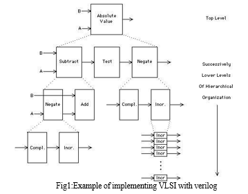
The design of hierarchical organization centers on the absolute value function, sometimes known as "Absolute Value." In this structure, the "Subtract" module is the most important module, and the "Test" component, which assesses the operation's success, comes next. Lower tiers of the hierarchy are successively comprised of functions like "Negate" and "Add," while custom modules like "Compl" and "Inor" carry out particular tasks inside the circuit. Complex digital circuit implementation is made easier by this hierarchical structure, which promotes modular and effective design. The essential mechanism of this system is the coupling of modules "A" and "B," which coordinates the data and signal flow required to compute the absolute value function. This helps to illustrate the complexities of VLSI design in handling intricate operations in integrated circuits.
B. Digital Filters
In order to alter or extract information from digital signals, digital filters are crucial parts of digital signal processing . its reaction to different frequency components of the incoming signal determines its classification. Two basic types of digital filters are Finite Impulse Response (FIR) filters and Infinite Impulse Response (IIR) filters. Due to their finite impulse response, FIR filters can only depend on a limited number of previous input samples to determine its output. They are appropriate for applications needing exact control over the frequency response of the filter because of their linear phase response and stability. IIR filters, on the other hand, have feedback, which produces an endless impulse response.
Because they are recursive, they usually provide more effective implementations than FIR filters for attaining comparable frequency responses. IIR filters, however, might have nonlinear phase response and stability problems. Numerous industries, including telecommunications, audio processing, picture processing, and biological signal analysis, use digital filters extensively. They are essential instruments for analyzing and modifying digital signals in a variety of real-world situations because to their efficacy and adaptability.
- FIR Filters
An example of a digital filter is a limited Impulse Response filter, which has an impulse response with a limited period. Each output sample in a FIR filter is the weighted sum of its input samples, with the weights being established by the filter coefficients. FIR filters are used for applications requiring accurate signal processing because they have a linear phase response and are intrinsically stable, in contrast to infinite impulse response (IIR) filters. FIR filters are widely used in image processing, biological signal analysis, telecommunications, and audio processing. Because of their finite impulse response feature, which makes them easily implementable with methods like convolution, they are useful tools for a variety of digital signal processing applications.
FIR filters provide fine-grained control over the features of frequency response. To satisfy the demands of various signal processing jobs, engineers can create FIR filters with certain frequency response profiles, such as low-pass, high-pass, band-pass, or band-stop. Furthermore, FIR filters maintain the phase connections in the input signal by offering linear phase response throughout the whole frequency range. This feature is very helpful in applications like audio and picture processing where phase distortion must be reduced to the lowest possible level.
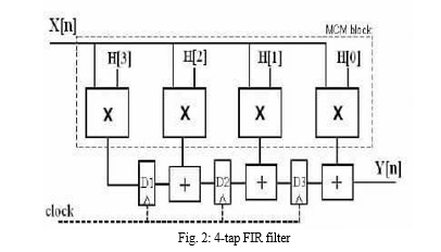
The system under discussion processes input signals using an adaptive filtering technique. The input signal, initially designated as x(n) , is first processed by an adjustable filter, which is represented by coefficients h_0 ,h_1 , and h_{x-2} , where x is the filter's length. Next, the input signal is convolution with the filter coefficients to get the output signal, y(n) . The echoed signal, d(n), is then produced by adding some of the input signal to the output signal. The error, e(n) , is then estimated by updating the coefficients using a recursive adaptive method. With the help of this adaptive technique, the filter can effectively adapt to changing conditions by dynamically adjusting its coefficients in response to the input signal and the predicted error.
C. Wallace Tree Multiplier
A popular high-speed parallel multiplier architecture in digital signal processing and other computationally demanding applications is the Wallace tree multiplier. By breaking down the multiplication process into smaller, easier-to-manage parts, it efficiently completes binary multiplication tasks.The inputs are first divided into groups of binary bits, usually three in the Wallace tree multiplier design. To produce partial products, a mix of full and half adders is used within each group. Then, these partial products are stacked in a binary tree-like hierarchical structure, where each level of the tree denotes a step of addition. Up until the final product is reached, the partial products are combined at each stage using a mix of full and half adders.
By dividing binary multiplication processes into smaller, parallelizable parts, the Wallace tree multiplier simplifies the process. First, inputs are divided into groups of three binary bits at a time. Partially product generation is applied to each group, whereby full and half adders are used to multiply individual bits. The phases of addition are represented by the different layers of this hierarchical consolidation of partial products, which resembles a binary tree structure. The incomplete products are combined at each phase, progressively building up to the finished result. When compared to traditional multiplication techniques, this parallelized approach lowers the critical path delay and improves the multiplier's speed and efficiency. A common computational application in digital signal processing and other fields where high-speed arithmetic operations are essential, offering significant performance improvements and scalability for demanding computational tasks.
III. PROPOSED METHOD
A Finite Impulse Response (FIR) filter's specifications cover a number of vital parts and functions that are necessary for the filter to work. Variables such as multiplicand A and multiplier B, which stand for the input signal and the filter coefficients, respectively, are initialized at the beginning. These variables define the properties of the filter's response to the input signal and function as the cornerstones for the following filtering operation.
After the initialization stage, the FIR filter calculates the partial products that result from multiplying each coefficient B by the multiplicand A. A partial product generator is used in this method to determine the intermediate outcomes for each multiplication operation. The final product, which represents the filtered output, is then by adding these partial products together.

The Wallace tree multiplier, which is an essential part of the FIR filter architecture, is used to quickly calculate the products A×B for each coefficient. By decreasing the amount of partial products and boosting computational efficiency, the Wallace tree multiplier optimizes the multiplication process and improves the FIR filter's overall performance.
Lastly, the FIR filter module checks that the final output is accurate, making sure that the filtered signal satisfies the criteria and maintains the intended frequency response characteristics. By precisely processing the input signal and attaining the intended filtering result, the FIR filter's effectiveness is verified through this verification procedure, which eventually confirms the filter's successful operation.
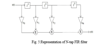
An N-tap Finite Impulse Response (FIR) filter's data flow diagram shows the processing steps required to filter an input signal x[n]. In the picture, each tap signifies a multiplication operation carried out between the input signal and a corresponding filter coefficient, b i, where b i varies from 0 to N, where N is the filter's length. The symbols with an encircling plus sign (?) are adders, which add together the output of these multiplications to provide the filtered output signal y[n]. The filtering action is clearly defined as a convolution between the input signal and the filter coefficients in the FIR filter's N-th order equation, meaning that the output at time instant n is the weighted sum of previous input samples.
The connection between the input and output signals in the frequency domain is represented by the linear invariant (LTI) FIR filter's transfer function, which is represented by H(z).

The frequency response characteristics of the FIR filter are captured by its transfer function H(z), which illustrates how the filter handles input signals at various frequencies. The FIR filter efficiently carries out a frequency-selective action, attenuating or amplifying particular frequency components in accordance with the filter's design, by convolving the filter coefficients with the input signal in the time domain. The output signal of the filter, represented by the Z-transform Y(z), sheds more light on the filter's behavior in the frequency domain by showing how it influences the input signal's various frequency components. For engineers creating filters for particular signal processing applications, it is essential to comprehend the transfer function and frequency response of the FIR filter. This is because it enables them to optimise filter performance in accordance with required frequency characteristics and design parameters.
Software and Hardware Environment
A complete development environment created especially for FPGA (Field-Programmable Gate Array) design and implementation is called Xilinx ISE 14.7. It provides a set of tools with an emphasis on Verilog-based projects for synthesizing, simulating, and implementing HDL (Hardware Description Language) designs. With support for the Spartan, Virtex, and Kintex Xilinx FPGA families, among others, Xilinx ISE gives designers the ability to build intricate digital systems that are intended for certain hardware platforms. Along with comprehensive functionality for timing analysis, optimisation, and debugging, the programme offers an easy-to-use interface for developing and debugging FPGA designs. When combined with IP (Intellectual Property) cores and Xilinx's wide selection of FPGA development boards, Xilinx ISE 14.7 provides a comprehensive solution for software and hardware development, enabling engineers to effectively design and implement FPGA-based solutions for a variety of applications.
IV. RESULTS
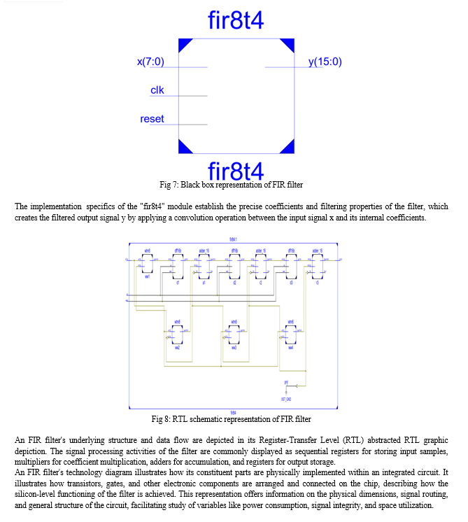
A Finite Impulse Response filter result's "black box" depiction usually captures the filter's operation without disclosing any of its internal workings. It acts as an abstraction so that users may only interact with the filter based on its input-output behavior, without having to comprehend the internal workings or specifics of its implementation. The input signal and the filtered output signal are represented by the input and output ports of the FIR filter, which are shown in this illustration as a functional block.
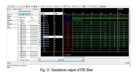
An eight-tap Finite Impulse Response (FIR) filter is represented by the "fir8t4" module. The process generates a 16-bit output signal y expressed as y(15:0) from an 8-bit input signal x (represented as x(7:0) . Clock clk and reset reset inputs are also included in the module to regulate the timing and startup of the filter operation. The module encapsulates the functionality of the FIR filter as a black box by abstracting its coefficients and internal structure.
V. FUTURE SCOPE
With continuous improvements in digital signal processing technology and applications, the future potential for FIR filters appears bright. The optimisation of FIR filter topologies is one way to advance in response to the growing need for faster and more efficient processing. To improve performance while lowering computing complexity, researchers are investigating cutting-edge strategies including distributed arithmetic, sparse FIR filters, and machine learning-based filter design approaches. Furthermore, there are new avenues for innovation due to the incorporation of FIR filters into cutting-edge technologies including artificial intelligence systems, 5G wireless communication, and the Internet of Things (IoT). The design and deployment of FIR filters will continue to progress due to research into adaptive filters, real-time implementation on reconfigurable hardware platforms, and application-specific optimisations.
Conclusion
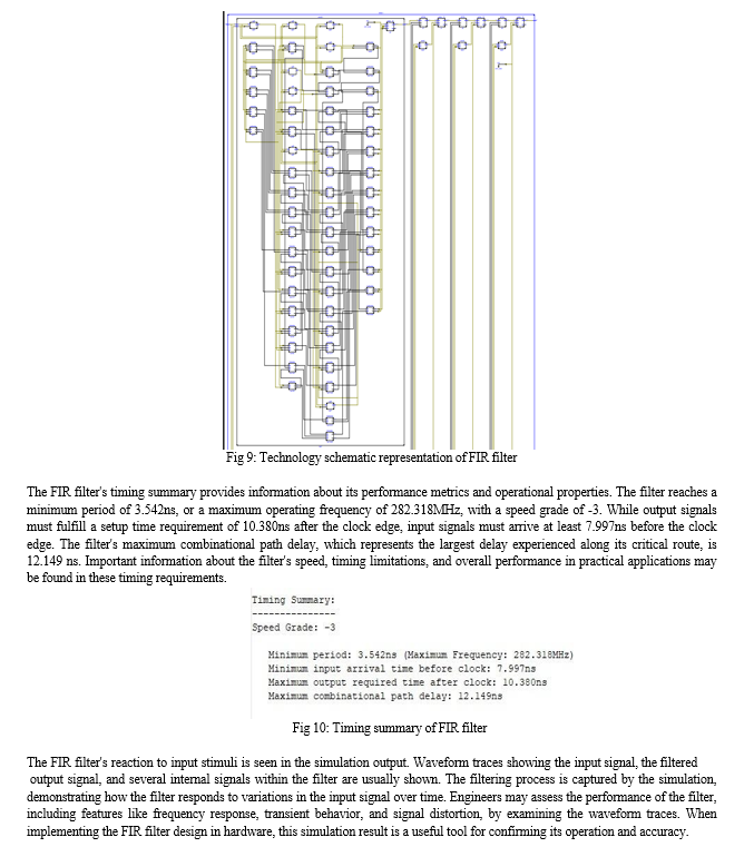
In summary, the Finite Impulse Response (FIR) filter is a crucial component of digital signal processing, providing adaptable features for a variety of uses. The FIR filter allows for precise control over frequency response characteristics and signal processing tasks by selectively modifying input signals based on a preset set of coefficients. Careful consideration of design characteristics and performance measures is necessary for its implementation, whether in software or hardware. Every element helps to comprehend and improve the filter\'s performance, from its black box depiction to its technological schematic and timing analysis. In the end, digital systems rely heavily on the FIR filter, which makes precise and efficient signal processing possible in a variety of contexts.
References
[1] R. Kumar, K. H. L. P. Prasad, B. Sriraj, and P. R. Rajasri, “FPGA Implementation of Systolic FIR Filter Using Single-Channel Method,” in 2023 13th International Conference on Cloud Computing, Data Science & Engineering (Confluence), Jan. 2023, pp. 215–220. doi: 10.1109/Confluence56041.2023.10048843. [2] V. Thamizharasan and N. Kasthuri, “FPGA implementation of high performance digital FIR filter design using a hybrid adder and multiplier,” Int. J. Electron., vol. 110, no. 4, pp. 587–607, Apr. 2023, doi: 10.1080/00207217.2022.2098387. [3] N. Chabini and R. Beguenane, “FPGA-Based Digital FIR Filters With Small Coefficients and Large Data Input,” in 2023 IEEE 13th Annual Computing and Communication Workshop and Conference (CCWC), Mar. 2023, pp. 0218–0221. doi: 10.1109/CCWC57344.2023.10099131. [4] V. Jamuna, P. Gomathi, and A. Arun, “Design and Implementation of FIR Filter Architecture Using High Level Transformation Techniques,” Indian J. Sci. Technol., vol. 11, no. 17, pp. 1–5, May 2018, doi: 10.17485/ijst/2018/v11i17/122769. [5] N. Udaya Kumar, U. Subbalakshmi, B. Surya Priya, and K. Bala Sindhuri, “VLSI Implementation of FIR Filter Using Different Addition and Multiplication Techniques,” 2018, pp. 483–490. doi: 10.1007/978-981-13-1936-5_51. [6] Q. Fu, G. Zhang, X. Wu, and S. Yan, “Optimized Design of FIR Filter Based On FPGA,” J. Phys. Conf. Ser., vol. 1626, no.1, p. 012143, Oct. 2020, doi: 10.1088/1742-6596/1626/1/012143. [7] L. Y. Akshitha V. Ramesh, Apeksha Ravi Kumar, Amulya S. Iyengar, “Implementation and Design of FIR Filters using Verilog HDL and FPGA,” 2020. [8] T. Dutta, R. M. Aich, S. Dhabal, and P. Venkateswaran, “Finite Impulse Response Filter Design using Grasshopper Optimization Algorithm and Implementation on FPGA,” in 2020 IEEE Applied Signal Processing Conference (ASPCON), Oct. 2020, pp. 313–317. doi: 10.1109/ASPCON49795.2020.9276711. [9] S. Chao, Q. Hui, S. Tong, M. Junzhi, Z. Yongjie, and D. Jianjun, “Design of FIR filter based on FPGA,” in 2020 IEEE 4th Information Technology, Networking, Electronic and Automation Control Conference (ITNEC), Jun. 2020, pp. 1691–1694. doi: 10.1109/ITNEC48623.2020.9084880. [10] A. K. Jameil, Y. A. Ahmed, and S. Albawi, “Efficient FIR Filter Architecture using FPGA,” Recent Adv. Comput. Sci. Commun., vol. 13, no. 1, pp. 91–98, Mar. 2020, doi: 10.2174/2213275912666190603115506. [11] Akshitha V Ramesh, Apeksha Ravi Kumar , Amulya S Iyengar, Lekha Yadav B “Implementation and Design of FIR Filters using Verilog HDL and FPGA” - An International Journal ISSN: 2566-932X, Vol. 4, Issue 5, August 2020 [12] G. Appala Naidu, “Implementation of Wallace tree multiplier using Xilinx with Verilog” – IERJ, E-ISSN No : 2454-991, Vol. 9, Issue 8, August 2023 [13] V. Thamizharasan, P. Pavithra “Design and analysis of Wallace tree multiplier using approximate full adder and Kogge stone adder” - ISO 3297:2007 Certified Vol. 11, Issue 3, March 2023 [14] Rozman Zakaria, F. Mohd Zaki “Digital Filter Design: Novel Multiplier Realization” - Journal of VLSI Circuits and Systems, ISSN: 2582-1458 Vol. 5, No. 2, 2023
Copyright
Copyright © 2024 V. Vittal Reddy , Udathu Jaya Madhuri , Vutukuri Sailaja , Zubera Farheen Khatun, Velpula Jagadish Kumar . This is an open access article distributed under the Creative Commons Attribution License, which permits unrestricted use, distribution, and reproduction in any medium, provided the original work is properly cited.

Download Paper
Paper Id : IJRASET60579
Publish Date : 2024-04-18
ISSN : 2321-9653
Publisher Name : IJRASET
DOI Link : Click Here
 Submit Paper Online

