Ijraset Journal For Research in Applied Science and Engineering Technology
- Home / Ijraset
- On This Page
- Abstract
- Introduction
- Conclusion
- References
- Copyright
Improving the SRAM Layout Design using Cadence Virtuoso
Authors: Nandhini R N, Venkat A K, Bitan De M
DOI Link: https://doi.org/10.22214/ijraset.2025.67014
Certificate: View Certificate
Abstract
The explosive growth in semiconductor technology has fuelled the need for high-speed, low-power, and small form factor memory solutions, and Static Random Access Memory (SRAM) is an indispensable part of contemporary integrated circuits. The conventional SRAM structures are beset with formidable power consumption, area, and stability trade-offs at different Process, Voltage, and Temperature (PVT) conditions. This paper introduces an optimized method for SRAM layout design with Cadence Virtuoso for 6T, 7T, 8T, and 10T SRAM cells to improve their performance in power-constrained and high-speed applications. The methodology uses layout optimization methods like transistor sizing, W/H ratio tuning, and power-conscious circuit design to obtain a balanced trade-off between read/write stability, leakage power minimization, and access speed enhancement. Detailed simulations are performed with varying PVT to analyse the effects of such variations on energy efficiency, area saving, and reliability. The results show that there is substantial improvement in the cell stability and power consumption and the optimized structures are suitable for next-generation high-performance and low-power computing devices. The paper presents a formal framework for SRAM layout optimization, providing valuable insights to memory designers working towards fulfilling the increasing demands of low energy embedded and high-performance computing applications.
Introduction
I. INTRODUCTION
Memory is an important aspect of modern-day electronic gadgets, which specifies the way they perform. Among all forms of memory, static random-access memory (SRAM) is recognized by its speed, minimum latency, and reliability. Compared to dynamic random-access memory (DRAM), where constant refreshment is needed, SRAM maintains data without needing additional power for refresh cycles. This makes it a great candidate for processor caches, embedded systems, and high-performance computing. However, despite all its advantages, SRAM has disadvantages too - it consumes more space and power than DRAM. With devices getting smaller and faster, optimizing SRAM efficiency has been a major goal in semiconductor technology. Optimizing SRAM design involves trading off three important parameters: speed, power, and area.
The access time of an SRAM cell is a function of how interconnects and transistors are structured access time must be minimized to remain in step with aggressive applications. Static as well as dynamic power dissipation must be kept to a minimum, particularly in battery-powered systems where energy efficiency is a big concern. Area optimization, in contrast, makes more memory available in a reduced area, reducing cost and improving overall device miniaturization. As technology continues to scale downward, finding the right balance among these factors becomes ever more challenging. Another serious challenge in SRAM design is alleviating process, voltage, and temperature (PVT) variation. With improvements in process and shrinking component size, these variations can affect memory stability and functionality as well as system performance, so SRAM cells must be designed to withstand various conditions successfully. To bridge such barriers, designers use electronic design automation (EDA) software such as Cadence Virtuoso. The software simulates and optimizes SRAM layouts with optimum transistor size, location, and interconnect structure. New design techniques and optimizations need to be done to turn future electronic devices more efficient and powerful.
II. LITERATURE REVIEW
SRAM has emerged as a key element of contemporary high-speed electronic systems and is used in microprocessors, embedded systems, and mobile phones. With the evolution of technology, there is an increasing need for smaller, faster, and lower power memory solutions. SRAM design optimization has emerged as a key area of concern in semiconductor technology, as designers struggle to balance access speed, power, area efficiency, and reliability. The capability to optimize these factors is of prime importance in providing high-performance memory solutions that satisfy the high demands of electronic devices today.
A few new design methods have been designed to overcome the problems and enhance SRAM efficiency with greater stability and reliability during various operating conditions. Transistor sizing is one of the most important elements of SRAM optimization that affects speed, power efficiency, and stability in a direct manner.
The use of larger transistors is more stable for cells and improves the noise margins but causes power dissipation to increase and area to be greater. Conversely, smaller transistors conserve area and power but may cause cell stability to be lower and access times to become slower. Successful SRAM design requires an ideal trade-off between them. Transistor placement in the SRAM array is another area that is very important. Optimal placement reduces interconnect delays and parasitic capacitances, resulting in increased access times and better area efficiency. With optimal transistor placement, designers can decrease the total layout area without compromising high-speed memory operation. This is especially critical for small devices like smartphones, IoT devices, and automotive systems, where space and power are important design factors. Layout design is equally critical to SRAM optimization. Effective layouts minimize the transistor usage while ensuring reliability and high-speed operation.
Cutting down the lengths of the interconnect and routing optimization decrease power consumption as well as contribute to overall efficiency of the chip. High-density SRAM configurations are necessary when there is considerable memory resource demanded in limited regions. Row/column sharing and making use of more compact transistors are ways to achieve peak memory density while not compromising speed. These techniques enable designers to pack more memory onto a single chip, cutting costs and enhancing overall device performance. The growing need for small, high-performance memory solutions in mobile devices, IoT devices, and automotive systems highlights the importance of ongoing advances in SRAM layout and density optimization. Power efficiency is also an important design consideration for SRAM, especially for battery-operated devices. Dynamic and static power dissipation need to be minimized to achieve maximum battery life and avoid heat generation. Techniques such as power gating, where unused regions of the SRAM are dynamically turned off, and adaptive voltage scaling, where supply voltage is scaled with workload, result in significant power savings. Static power dissipation due to leakage currents is another key low-power SRAM design challenge. Use of low-leakage transistors and optimal threshold voltages can lower static power consumption and make SRAM more efficient for energy-saving applications. As the development of mobile and wearable electronics advances, embedding power-conversation techniques into SRAM design is more essential to optimize performance and efficiency.
Ensuring robustness against process, voltage, and temperature (PVT) variations is another issue with SRAM design. With semiconductor technology decreasing, SRAM cells are increasingly affected by changes in the environment and need to have noise margins improved. Various techniques like expanding spacing between sensitive nodes, using shielding structures, and applying decoupling capacitors reduce the problem of noise and increase reliability. Such approaches make SRAM cells operate in a stable manner and at an operational condition that is insensitive to changes in conditions, less likely to corrupt data and induce errors. For those applications demanding high reliability, such as in the case of automotive systems and medical devices, adequate noise margins need to be sustained to achieve dependable performance. Breakthroughs in FinFET technology have already greatly increased scalability and power savings in SRAM designs. SRAM cells that use FinFET based technologies provide superior control of electrostatics, lowered leakage current, and increased energy efficiency than legacy planar transistors. This facilitates further miniaturization without reducing performance, so FinFET based SRAM is an appropriate option for high-density memory applications. Low-power design methods in leading CMOS technologies, like sub-threshold operation and supply voltage scaling, are also gaining relevance in lowering power consumption without sacrificing performance levels. These schemes assist in obtaining power-efficient SRAM designs, especially for battery-operated devices and mobile platforms where power limitations are a chief concern. As the demand for high-density, low-power, and high-performance memory solutions increases, SRAM optimization continues to be a research and development priority area. With the implementation of cutting-edge design approaches, novel transistor structures, and power reduction strategies, SRAM technology can be optimized to fulfill the requirements of future electronic products. The use of FinFET technology, low-power design styles, and power-efficient layout methodologies guarantees SRAM as a critical building block in current electronic systems, driving computing, mobile computing, and beyond innovation.
III. PROPOSED DESIGN
The proposed design of the paper focuses with the designing the layout for a 6T SRAM cell with a static power consumption of 30–50 nanowatts and dynamic power of 400–1000 nanowatt per cell. Simulations were performed by using Cadence Virtuoso software which is to accomplish the above results, and it was found that the design had noticeable improvements in power efficiency and overall layout performance. The power consumption must be reduced to improve its performance and decrease the layout size. The size of the SRAM cell is defined by the width-to-height (W/H) ratio of the layout. The exact power consumption is determined by the equations:
A. Static Power Consumption
PStatic = V DC × I D
Where V DC = Power supply voltage I D = Leakage current
B. Dynamic Power Consumption
PDynamic = C Eff × F Clk × V 2 DC
Where C Eff = Effective Capacitance,
F Clk = Clock Frequency
C. Width To Height Ratio
WH ratio = Width of the layoutHeight of the layout
The layout is created through an iterative process of testing 10T, 8T, and 7T SRAM cells. The iterative design process and the design parameters for each iteration are given below:
1) Iteration A: 10 T SRAM LAYOUT
In this iteration, we simulated a 10T SRAM cell layout with a power supply voltage of 1.8 V. The results of the simulation were determined by the following parameters in Table 1, Fig 1,2,3.
Table 1: Design parameters in Iteration A
|
Static power consumption |
Dynamic power consumption |
Width to Height (W/H) ratio
|
|
50 - 80 nanowatts per cell |
600 – 1500 nanowatts per cell |
T1, T2 – 1.5:1 to 1.8:1 T3, T4 – 2.8:1 to 3.2:1 T5, T6 – 3.5:1 to 4.5:1 T7, T8 – 1.2:1 to 2:1 T9, T10 – 1.4:1 to 2.1:1 |
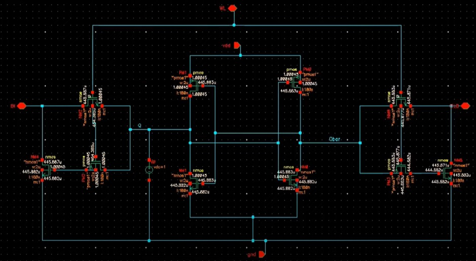
Fig. 1 SRAM design of 10 Transistors layout
Q vs Q B plot
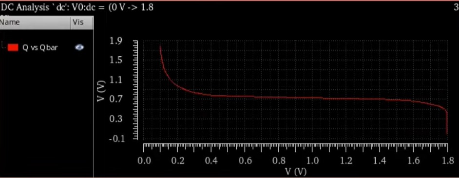
Fig. 2 DC analysis plot of Q
Q B vs Q plot
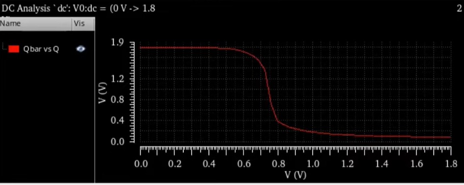
Fig. 3 DC analysis plot of Qb
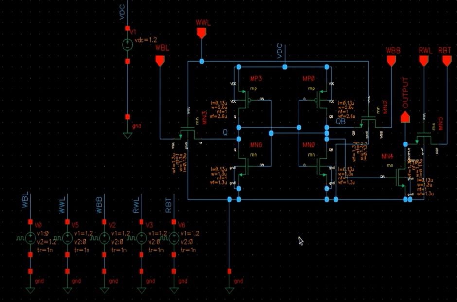
Fig. 4 SRAM design of 8 Transistors layout
2) Iteration B: 8 T SRAM LAYOUT
In this iteration, we simulated an 8T SRAM cell layout with a power supply voltage of 1.8 V. The results of the simulation were determined by the following parameters in Table 2, Fig 4,5,6.
Table 2: Design parameters in Iteration B
|
Static power consumption |
Dynamic power consumption |
Width to Height (W/H) ratio
|
|
45 – 75 nanowatts per cell |
550 – 1300 nanowatts per cell |
T1, T2 – 1.4:1 to 1.6:1
T3, T4 – 2.6:1 to 3:1
T5, T6 – 3.2:1 to 4:1
T7, T8 – 1.1:1 to 2:1 |
Q vs Q B plot
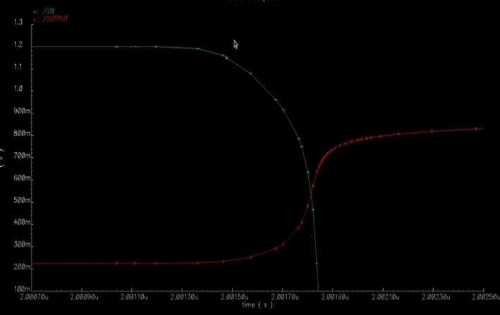
Fig. 5 DC analysis plot of Q
Q B vs Q plot
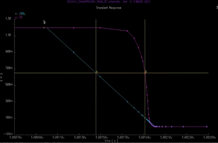
Fig. 6 DC analysis plot of Qb

Fig. 7 SRAM design of 7 Transistors layout
3) Iteration C: 7T SRAM LAYOUT
In this iteration, we simulated an 7T SRAM cell layout with a power supply voltage of 1.8 V. The results of the simulation were determined by the following parameters in Table 3, Fig 7,8,9.
Table 3: Design parameters in Iteration C
|
Static power consumption |
Dynamic power consumption |
Width to Height (W/H) ratio
|
|
45 – 75 nanowatts per cell |
600 – 1300 nanowatts per cell |
T1, T2 – 1.3:1 to 1.5:1
T3, T4 – 2.4:1 to 2.8:1
T5, T6 – 3:1 to 3.8:1
T7 – 1.1:1 to 1.8:1 |
Q vs Q B plot

Fig. 8 DC analysis plot of Q
Q B vs Q plot
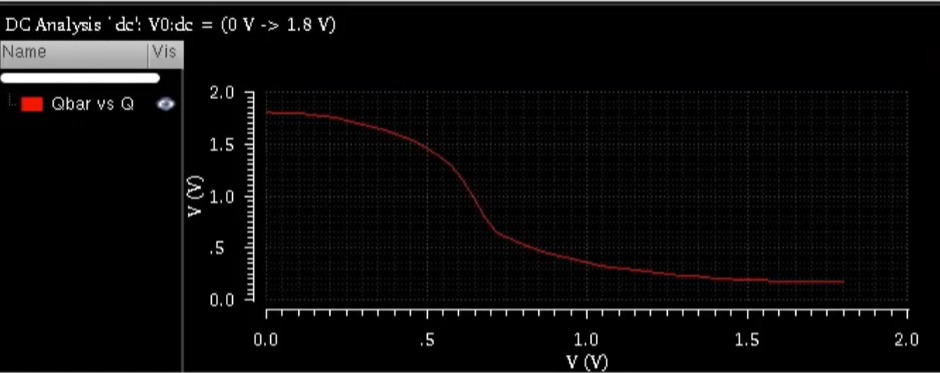
Fig. 9 DC analysis plot of Qb
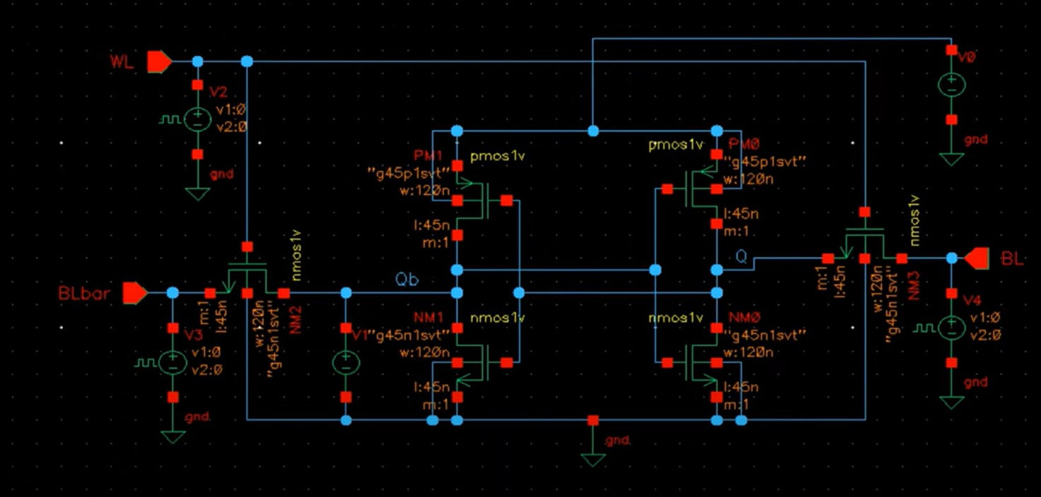 Fig. 10 SRAM design of 6 Transistors layout
4) Iteration D: 6 T Sram Layout
In this iteration, we simulated an 8T SRAM cell layout with a power supply voltage of 1.8 V. The results of the simulation were determined by the following parameters in Table 4, Fig 10,11,12.
Table 4: Design parameters in Iteration D
|
Static power consumption |
Dynamic power consumption |
Width to Height (W/H) ratio
|
|
30 – 50 nanowatts per cell |
400 – 1000 nanowatts per cell |
T1, T2 – 1.2:1 to 1.5:1
T3, T4 – 2.5:1 to 3:1
T5, T6 – 3:1 to 4:1 |
Q vs Q B plot
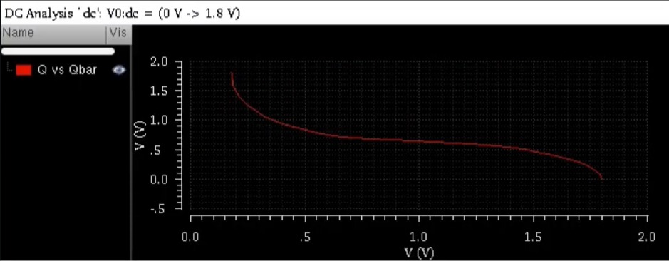
Fig. 11 DC analysis plot of Q
Q B vs Q plot

Fig. 12 DC analysis plot of Q
The design calculations for the proposed SRAM layout are as follows: The supply voltage (Vdc) is set at 1.8 V, with an effective capacitance of 5 × 10? F. The clock frequency is 246 × 10? Hz, and the leakage current is measured at 22.2 mA. These parameters were carefully selected to optimize the power efficiency, stability, and performance of the design.
IV. RESULTS
The proposed layout was designed, and the simulation was done by using the Cadence Virtuoso software. The simulated results of a 6T SRAM cell layout are discussed in this paper. The results of the parameters of different iterations are compared.
Table 5. Comparison of SRAM layout parameters - power consumption
|
Performance measure
|
10T SRAM CELL |
8T SRAM CELL |
7T SRAM CELL |
6T SRAM CELL
|
|
Static power consumption
|
50 – 80 nano watts per cells |
45 – 75 nano watts per cells |
45 – 75 nano watts per cells |
30 – 50 nano watts per cells
|
|
Dynamic power consumption
|
600 – 1500 nano watts per cells |
550 – 1300 nano watts per cells |
600 – 1300 nano watts per cells |
400 – 1000 nano watts per cells
|
Table 6. Comparison of SRAM layout parameters – w/h ratio with existing works of different no. of transistors design
|
Transistor sizing
|
10T SRAM CELL |
8T SRAM CELL |
7T SRAM CELL |
6T SRAM CELL
|
|
T1, T2
|
1.5:1 to 1.8:1 |
1.4:1 to 1.6:1 |
1.3:1 to 1.5:1 |
1.2:1 to 1.5:1
|
|
T3, T4
|
2.8:1 to 3.2:1 |
2.6:1 to 3:1 |
2.4:1 to 2.8:1 |
2.5:1 to 3:1
|
|
T5, T6
|
3.5:1 to 4.5:1 |
3.2:1 to 4:1 |
3:1 to 3.8:1 |
3:1 to 4:1
|
|
T7, T8
|
1.2:2 to 2:1 |
1.1:1 to 2:1 |
1.1:1 to 1.8:1 |
-
|
|
T9, T10
|
1.4:1 to 2.1:1 |
- |
- |
- |
From the design of 10T SRAM cell, we have obtained the power consumption as 50 – 80 nanowatts per cell, then after implementation of 8T SRAM cell we obtained a power consumption as 45 – 75 nanowatts per cell.
Furthermore, the implementation of 7T has the same power consumption without variation. After implementation of 6T SRAM cell layout it is observed that the power consumption is around 30 – 50 nanowatts per cell which is capable of reduced W/H ratio layout.
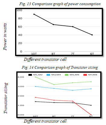
The simulation showcases good performance in decrease in power consumption and transistor sizing. This provides a better performance of different layout design along with the application.
Conclusion
This work provides an improved approach to the design and simulation of SRAM cell layouts using power efficiency, area reduction, and stability for different configurations. From Cadence Virtuoso, we have achieved static power dissipation of 30–50 nanowatts and dynamic power of 400–1000 nanowatts per cell, demonstrating the efficacy of modern layout techniques and transistor sizing to improve SRAM performance. With precise optimization of the width-to-height aspect ratio, the design was minimized without compromising stability and reliability under changing conditions of operation. The presented design process gives a guideline to be followed in future optimizations, striking a balance between power efficiency and performance by means of enhanced transistor sizing and layout density. Future upgrades may involve the migration to next-generation technology such as FinFET or GAAFET with improved electrostatic control and leakage reduction to allow for even more scalable and high-density SRAM cells. Moreover, the improvement of the noise margin via node shielding and spacing optimization in the layout would further enhance the stability of design, especially in high-speed and low-voltage applications. Another path that is being actively explored is the integration of process variability analysis, allowing SRAM\'s performance to be consistent as SRAM scales downward to smaller technology nodes. A hybrid SRAM architecture can also potentially eliminate read/write contention, resulting in even better efficiency and reliability. Optimizations such as these provide the platform for next-generation SRAM implementations to meet modern electronic systems\' increasing demands of high performance and power efficiency.
References
[1] Kuo, Y. C. P., \"Transistor Sizing for SRAM Cells,\" IEEE Journal on VLSI Systems, 2019. [2] Choi, M. S., et al., \"Optimal Transistor Placement for High-Performance SRAM Arrays,\" IEEE Journal on Circuits and Systems II: Express Briefs, 2020. [3] Lee, R. S. H. B., et al., \"Efficient Layout Design for SRAM Arrays,\" IEEE Journal of Solid-State Circuits, 2019. [4] Liu, T. H. W., et al., \"High-Density SRAM Design Techniques,\" IEEE Journal on VLSI Systems, 2020. [5] Koo, J. B. T., et al., \"Power-Efficient SRAM Design: A Review,\" IEEE Journal on Circuits and Systems I: Regular Papers, 2019. [6] Smith, M. A. J., et al., \"Enhancing SRAM Noise Margins through Layout Techniques,\" IEEE Journal on Circuits and Systems II: Express Briefs, 2021. [7] Liu, T. H. W., et al., \"Fin FET SRAM Design for High-Density Integration,\" IEEE Journal of Solid-State Circuits, 2021. [8] Lee, S. H., et al., \"Design Techniques for Low-Power SRAM in Advanced CMOS Technology,\" IEEE Journal on VLSI Systems, 2021. [9] Najafi, D., et al., \"Enabling Normally-off In-Situ Computing with a Magneto-Electric FET-based SRAM Design,\" arXiv:2312.05212, 2023. [10] Wang, D., et al., \"TL-SRAM-CIM: Ultra-High-Density Three-Level ReRAM-Assisted Computing-in-SRAM with DC-Power Free Restore and Ternary MAC Operations,\" arXiv:2307.02717, 2023. [11] Chen, Y., et al., \"FAST: A Fully Concurrent Access Technique to All SRAM Rows for Enhanced Speed and Energy Efficiency in Data-Intensive Applications,\" arXiv preprint arXiv:2205.11088, 2022. [12] Wang, X., et al., \"A 137.5 TOPS/W SRAM Compute-in-Memory Macro with 9-b Memory Cell-Embedded ADCs and Signal Margin Enhancement Techniques for AI Edge Applications,\" arXiv:2307.05944, 2023. [13] Chen, Y., et al., \"Energy-Efficient High Bandwidth 6T SRAM Design on Intel 4 CMOS Technology,\" IEEE Journal of Solid-State Circuits, 2021. [14] Rathi, N., et al., \"Architectural Designs and Performance Analysis of Adiabatic-based SRAM Cells,\" 2023 IEEE Devices for Integrated Circuit (DevIC), 2023.
Copyright
Copyright © 2025 Nandhini R N, Venkat A K, Bitan De M. This is an open access article distributed under the Creative Commons Attribution License, which permits unrestricted use, distribution, and reproduction in any medium, provided the original work is properly cited.

Download Paper
Paper Id : IJRASET67014
Publish Date : 2025-02-18
ISSN : 2321-9653
Publisher Name : IJRASET
DOI Link : Click Here
 Submit Paper Online

