Ijraset Journal For Research in Applied Science and Engineering Technology
- Home / Ijraset
- On This Page
- Abstract
- Introduction
- Conclusion
- References
- Copyright
Low Power Design of Efficient Wireless Sensor Node
Authors: Vighneshkumar Uttarkar, Poornima G
DOI Link: https://doi.org/10.22214/ijraset.2024.58844
Certificate: View Certificate
Abstract
The escalating demand for rapid, efficient System on Chip (SoC) designs has intensified the need for low-power solutions, particularly in Wireless Sensor Nodes reliant on battery power. This research centers on leveraging clock gating to curtail dynamic power usage in an 8-bit Arithmetic and Logic Unit (ALU). Employing the Hans-Carlson Adder for addition and a 4x4 approximation multiplier, the ALU processes data from a humidity sensor module. Simulations using Xilinx Vivado reveal a substantial 65–73% reduction in power consumption at higher frequencies. This ALU, adept at minimizing power, emerges as a viable processing element for energy-sensitive sensor node applications, ensuring prolonged operational longevity.
Introduction
I. INTRODUCTION
Applications for wireless sensor networks (WSN) include monitoring of medical conditions, industrial inspection, military surveillance, and environmental parameter sensing. Sensors, radio communication, and a microprocessor powered by a small power source, such as a storage battery, are the basic components of WSN nodes. To increase the lifespan of the sensor node, the total amount of energy needed for the node should be kept to a minimum because radio communication uses a lot of it. Between 100 and 3000 is the range of the communication-to-computation energy price ratio.
The low power ALU design for the processing component used in the wireless sensor node is included in the scope. Clock gating technique is used to cut down on dynamic power use, which then cuts down on switching power. To further reduce computation time, a parallel prefix adder similar to the Han-Carlson adder is included. Additionally, the multiplier helps reduce the amount of space needed. By doing so, the extra space used by the clock gating circuits will be balanced. This can use in many application such as in the radio communication system.
Radio modules on wireless sensor nodes allow for communication. If two nodes are able to send and receive data back and forth, then they are directly connected. A mathematical model that measures the direct connectedness between sensor nodes is called a sensor communication model, also sometimes referred to as a transmission model. Preferably in the applications such as key distribution, location estimation, processor sensor web, sensor network query, wireless power line sensor, and telemetry. Methodology of the project is shown in below figure 1 proposed designed blocks.
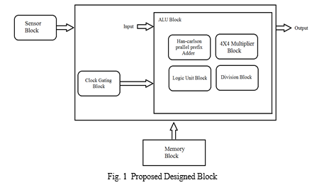
A Clock Gated Arithmetic and Logic Unit are designed with a low power. The ultimate technique to get desired gain in power is clock-gating. A Clock Gated Arithmetic and Logic Unit are designed with a low power. The ultimate technique to get desired gain in power is clock-gating. Han-Carlson Adder: It is a parallel prefix adder. Parallel Prefix adder is utilized as it is one of the high speed adders.
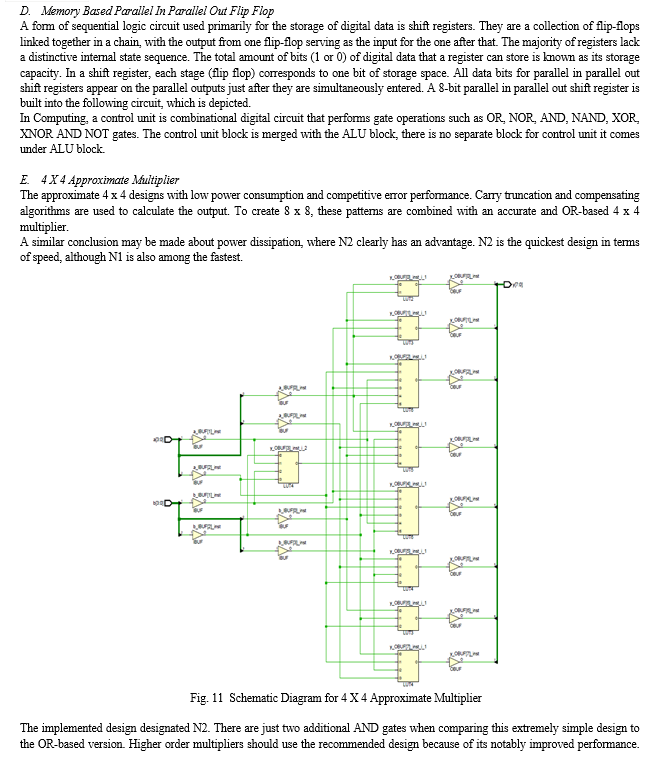
4 X 4 approximates Multiplier: The two novel 4x4 approximate multiplier designs with minimal power requirements and competitive error performance. The multipliers uses shift and add algorithm and this 4X4 multiplier uses 16 AND gates, 4 half adders & 8 full adders so total 12 adders.
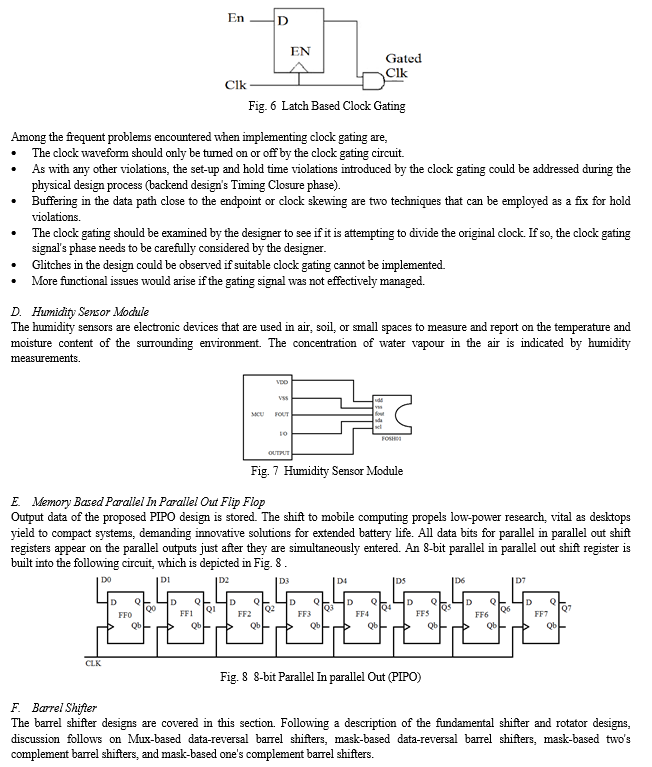
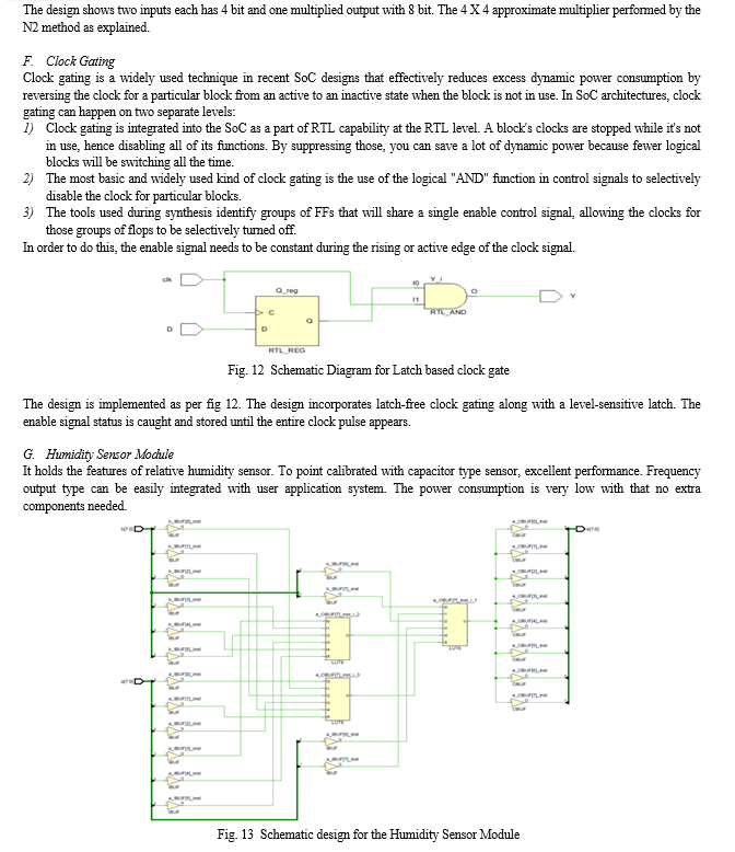
Clock gating circuit: The ultimate technique to get desired gain in power. Clock gating refers to activating the clocks in a logic block only when there is work to be done. The clock is gated using a Latch-based clock gating circuit that generates an enable signal in line with the opcodes.
II. LITERATURE SURVEY
- Comparative Analysis of Adders Parallel-Prefix Adder for Their Area, Delay and Power Consumption - This paper introduces Parallel Prefix Adders (PPA) as a faster alternative to ripple carry adders (RCA). The study compares four 8-bit PPAs (LFA, KSA, BKA, HCA) against Ladner-Fischer, Kogge-Stone, Bent-Kang, Han-Carlson, and Parallel Prefix adders, assessing their performance in terms of area, delay, and power for comprehensive analysis and evaluation. The findings show that, in terms of area, latency, and power, the suggested Han-Carlson adder Parallel-Prefix Adder is superior to the other three types of Parallel-Prefix adders.
- Approximate Recursive Multipliers Using Low Power Building Blocks - This paper explores approximate computing for power-efficient binary multipliers, presenting two 4x4 approximate multipliers with carry manipulation. Composing 8x8 designs with varied error-performance trade-offs, they outperform state-of-the-art designs, reducing power consumption and silicon area by 46% while maintaining 81% higher accuracy.
- Simulation of Enhanced Pulse Triggered Flip Flop with High Performance Application - In this paper, Flip-flops, crucial in System on Chip (SOC) designs, contributes significantly to power consumption. This paper proposes an Enhanced Pulse Triggered Flip Flop (D-FF) for applications like 4-bit PIPO, 4-bit SISO, and 3-bit Asynchronous ripple counter, aiming to minimize power dissipation. Performance evaluations are conducted using TSMC 180nm technology.
- Development of Processor Engine for FPGA Based Clock Gating and Performing Power Analysis - In this paper, In addressing challenges posed by Moore's Law scaling for high-performance, low-power processors, this paper focuses on reducing dynamic power dissipation through latch-free clock gating. Applied to a 32-bit Arithmetic and Logic unit, the functional unit-enabled approach demonstrates an average power reduction of 65.35% and 52.24% for lower and higher frequencies, respectively.
- Clock Gating A Power Optimizing Technique for VLSI Circuits – In this paper, Clock gating, a power-saving method utilized in the Pentium 4 and subsequent processors, involves activating clocks in a logic block only when needed to conserve power. This paper explores various clock gating techniques for power optimization in VLSI circuits at the RTL level, addressing challenges associated with applying these techniques effectively.
III. METHODOLOGY
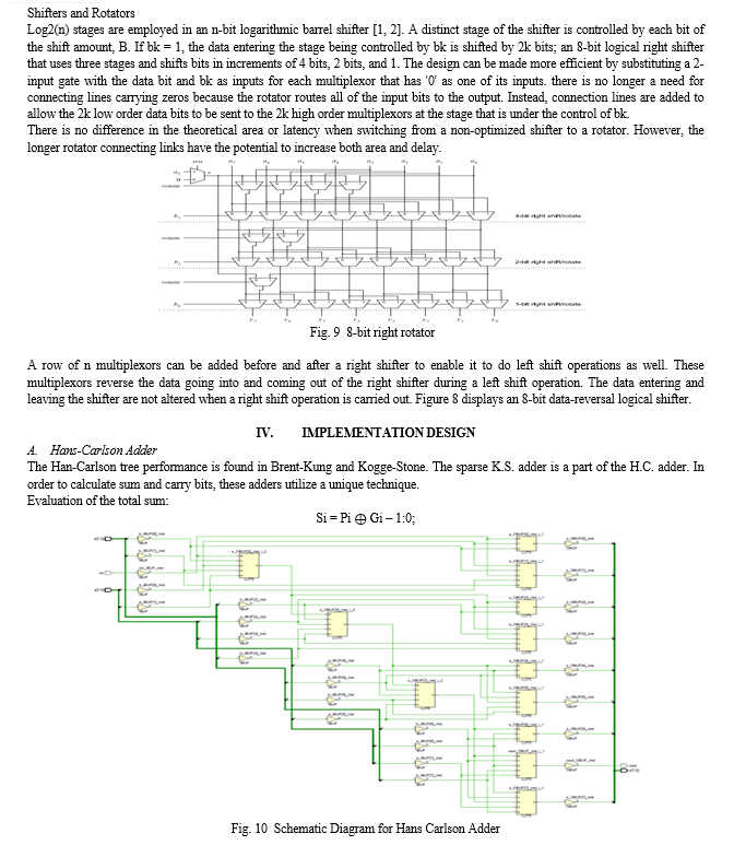
Design low-power ALU employing with clock gating. The Arithmetic and Logic Unit, a collection of registers, a control unit, and other components make up the bulk of the basic processor design.
A. 4 X 4 Approximate Multiplier
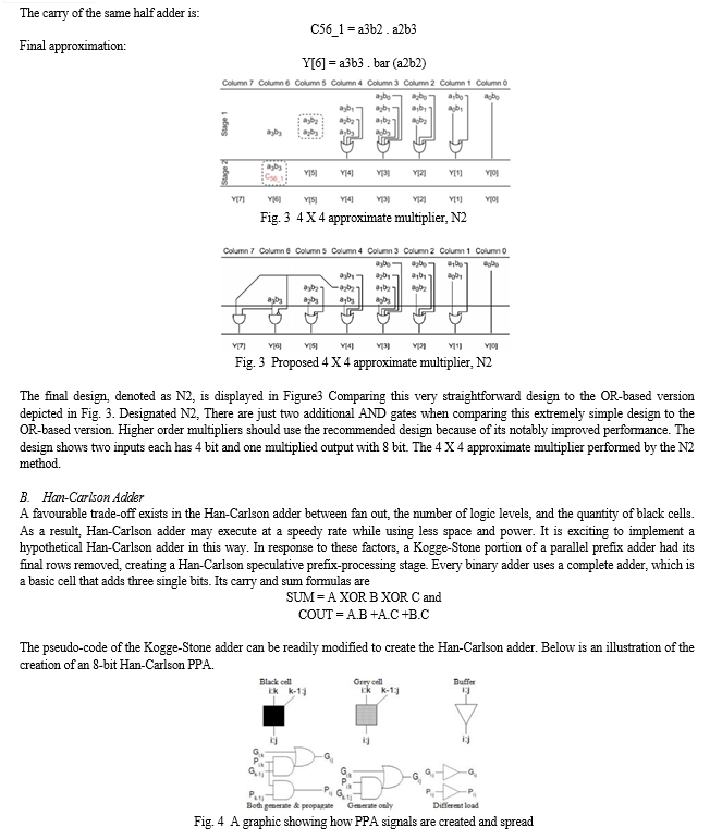
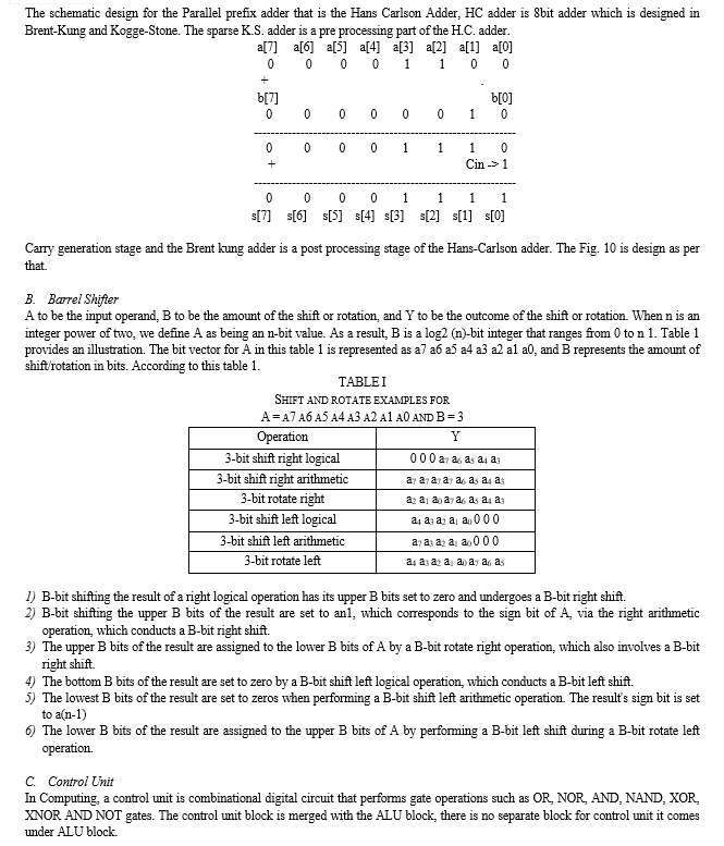
In block of ALU the one of the block is multiplier Fig. 1. The approximate 4 X 4 designs with low power consumption and competitive error performance. Carry truncation and compensating algorithms are used to calculate the output. To create 8 x 8, these patterns are combined with an accurate and OR-based 4 X 4 multiplier. The circuit in Fig. 2 serves as the foundation for further simplification in the suggested armature.
The 4 x 4 approximate multiplier, while two HAs are used to compute the three most significant outputs, OR gates are used to approximate the five least significant outputs. the initial architectural blueprint for the suggested N2 concept.
The first step is to replace the half-adder's XOR gate in column 5 with an OR gate.
Y[5]= a3b2 + a2b3


Conclusion
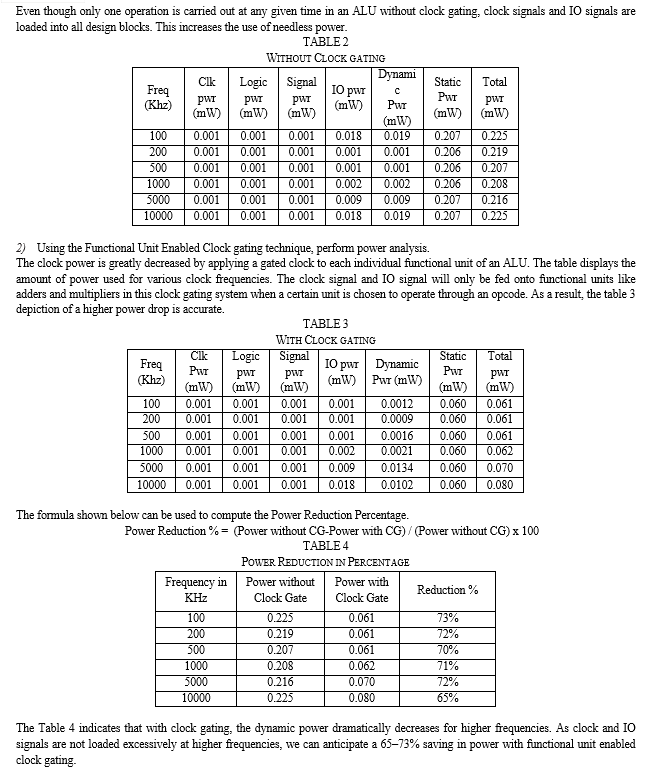
8-bit ALU is given a clock gating system, waveforms are simulated, and power analysis is carried out using the Xilinx Vivado Power Analyzer 18.2 Suite. The ALU block with memory storage for the data output that is parallel in parallel out design with the sensor of humidity HH10D makes up a large portion of the full on chip design. For the design of a multiplier in an ALU, the 4x4 approximation is utilized. For the adder block with adding logic control unit and division with minimal area and low power consumption, Hans Carlson parallel prefix adder is employed. Without clock gating and Enabled Clock gating are the two distinct clock gating approaches that are used. For the latter technique, the power drop is more clearly seen. The power reduction is less for lower frequencies, as we saw that for 100MHz and 200MHz, it ranges between 50 and 60%, however for higher frequencies, like 500MHz and 1GHz, it ranges between 65 and 73%, and the power reduction is large. This is due to the fact that as the frequency rises, the superfluous loading of clock and IO signals, which accounted for the majority of dynamic power consumption, is considerably reduced. The larger power decrease offsets the additional space needed for clock gating circuitry. Clock gated ALUs are recommended for wireless sensor applications where power conservation is a major concern due to the large power savings. A. Future Scope The main motivation for the proposed study is ALU power reduction. The processor element and this ALU can be combined to create a low power processor. When creating much more efficient processor architecture, speed of computations must also be taken into account in addition to power. By creating adders and multipliers that are significantly faster, the speed can be increased. These clock gating circuits take up more space. The multiplier was created with low-space-consuming folded tree architecture in order to get around this. However, in order to accomplish this, the multiplier\'s speed has to be reduced. Therefore, this job can be improved by creating a quick multiplier that also uses less space.
References
[1] Sharath, M., Poornima, G. (2020). Design of Energy Efficient ALU Using Clock Gating for a Sensor Node. In: Auer, M., Ram B., K. (eds) Cyber-physical Systems and Digital Twins. REV2019 2019. [2] C. Walravens and W. Dehaene, \"Low-Power Digital Signal Processor Architecture for Wireless Sensor Nodes,\" in IEEE Transactions on Very Large Scale Integration (VLSI) Systems, vol. 22, no. 2, [3] C. S. Jasmin and A. P. Mathew, \"Power efficient comparator architecture for wireless sensor nodes,\" 2016 International Conference on Emerging Technological Trends (ICETT), Kollam, India, 2016, [4] A. Dhanunjaya Reddy, \" Area Efficient Speculative Han-Carlson Adder\", International Journal of Scientific Research in Science and Technology(IJSRST), Volume 3, Issue 7 2017. [5] E. Zacharelos, I. Nunziata, G. Saggese, A. G. M. Strollo and E. Napoli, \"Approximate Recursive Multipliers Using Low Power Building Blocks,\" in IEEE Transactions on Emerging Topics in Computing, vol. 10, no. 3, 2022. [6] D. -H. Le, N. Sugii, S. Kamohara, X. -T. Nguyen, K. Ishibashi and C. -K. Pham, \"Design of a low-power fixed-point 16-bit digital signal processor using 65nm SOTB process,\" 2015 International Conference on IC Design & Technology (ICICDT), Leuven, Belgium, 2015. [7] J. Shinde and S. S. Salankar, \"Clock gating — A power optimizing technique for VLSI circuits,\" 2011 Annual IEEE India Conference, Hyderabad, India, 2011. [8] C., Bhaskar & Jathar, Vikas. (2016). Development of processor engine for FPGA based clock gating and performing power analysis. [9] E. Zacharelos, I. Nunziata, G. Saggese, A. G. M. Strollo and E. Napoli, \"Approximate Recursive Multipliers Using Low Power Building Blocks,\" in IEEE Transactions on Emerging Topics in Computing, vol. 10, no. 3 2022. [10] Dr. V. Sidharthan, M. Prasannakumar, \" Comparative Analysis of Adders Parallel-Prefix Adder for Their Area, Delay and Power Consumption\", International Journal of Scientific Research in Science and Technology(IJSRST) Volume 4, Issue 5-2018. [11] Nehru, Kamla et al. “Design of 64-bit low power parallel prefix VLSI adder for high speed arithmetic circuits.” 2012 International Conference on Computing, Communication and Applications (2012): 1-4. [12] Nguyen, Xuan-Thuan & Bui, Trong-Tu & Huynh Huu, Thuan & Pham, Cong-Kha & Le, Duc Hung. (2013). An ASIC Implementation of 16-bit Fixed-point Digital Signal Processor. Journal of Science and Technology (Special Issue). 51. 282-289. [13] R. Kulkarni and S. Y. Kulkarni, \"Power analysis and comparison of clock gated techniques implemented on a 16-bit ALU,\" International Conference on Circuits,Communication, Control and Computing, Bangalore, India, 2014, pp. 416-420, doi:10.1109/CIMCA.2014.7057835. [14] G. Shrivastava and S. Singh, \"Power Optimization of Sequential Circuit Based ALU Using Gated Clock & Pulse Enable Logic,\" 2014 International Conference on Computational Intelligence and Communication Networks, Bhopal, India, 2014, pp.1006-1010, doi: 10.1109/CICN.2014.212. [15] Singh, maneesh & kumar, rajeev. (2015). Ijesrt international journal of engineering sciences & research technology simulation of enhanced pulse triggered flip flop with high performance applications. International journal of engineering sciences & research technology. 489-493. [16] C., Bhaskar & Jathar, Vikas. (2016). Development of processor engine for FPGA based clock gating and performing power analysis. 1-5.10.1109/ICCUBEA.2016.7860113. [17] E. Zacharelos, I. Nunziata, G. Saggese, A. G. M. Strollo and E. Napoli,\"Approximate Recursive Multipliers Using Low Power Building Blocks,\" in IEEE Transactions on Emerging Topics in Computing, vol. 10, no. 3, pp. 1315-1330, 1 July-Sept. 2022, doi: 10.1109/TETC.2022.3186240. [18] Dr. V. Sidharthan, M. Prasannakumar, \" Comparative Analysis of Adders Parallel-Prefix Adder for Their Area, Delay and Power Consumption\", International Journal of Scientific Research in Science and Technology(IJSRST), Print ISSN :2395-6011, Online ISSN : 2395-602X, Volume 4, Issue 5, pp.353-357, March-April-2018. [19] https://docs.xilinx.com/v/u/2018.2-English/ug893-vivado-ide [20] https://worldofdatasheets.com/
Copyright
Copyright © 2024 Vighneshkumar Uttarkar, Poornima G. This is an open access article distributed under the Creative Commons Attribution License, which permits unrestricted use, distribution, and reproduction in any medium, provided the original work is properly cited.

Download Paper
Paper Id : IJRASET58844
Publish Date : 2024-03-07
ISSN : 2321-9653
Publisher Name : IJRASET
DOI Link : Click Here
 Submit Paper Online

