Ijraset Journal For Research in Applied Science and Engineering Technology
- Home / Ijraset
- On This Page
- Abstract
- Introduction
- Conclusion
- References
- Copyright
Design of Low Power Double Tail Dynamic Comparator
Authors: Poornima G, Soundarya N
DOI Link: https://doi.org/10.22214/ijraset.2024.63031
Certificate: View Certificate
Abstract
Dynamic regenerative comparators are being used more and more to enhance power and speed economy in analog-to-digital converters. These converters must be extremely low-power, area-efficient, and high-speed. In this case, the DCs (DC) power is analyzed. A new DC is suggested, modifying the traditional double-tail comparator circuit for quick and low-power functioning even at low supply voltages, in accordance with the analysis that has been provided. Little transistors are added, and the construct is kept simple. Additionally, a new DC in line with on the suggested double-tail topology is provided; this comparator doesn\'t need a boosted voltage or excessive transistor stacking. Additionally, a latest DC is narrated that it doesn’t not require boosted voltage or the stacking of an excessive number of transistors, based on the double-tail structure that has been proposed. Time for Latch delay is greatly decreased by just incorporating a small number of minimum-size transistors into the traditional double-tail DC. Comparing this improvement to the traditional DC and double-tail comparator, significant power reductions are also achieved. The construction of a distinct input and cross-coupled stage is the foundation of the double-tail DC. Fast functioning across a broad common-mode and supply voltage scale is made possible by this separation. This work presents a thorough investigation of DC delays for a variety of topologies. The probe results are validated by the results of simulation in 90 nanometer CMOS technology. It is demonstrated that the DC has a much lower power consumption. At voltage, the comparator\'s maximal clock frequency is raised to 2.5 Hz, consuming 6.76 ?W in the process. Index Terms – Dynamic Comparator, Double tail DC, latch delay, low power operation.
Introduction
I. INTRODUCTION
The entire dynamic and static power consumption of an integrated circuit can be reduced by employing a range of strategies and procedures together referred to as low power design. Reducing the consumption of power of each individual component is the goal of low power VLSI design, which lowers the overall power consumed. The dynamic power derived from switching and short-circuit power, whereas the static power comes from leakage current flowing along a transistor. Lowering the individual power components as much as feasible will lower the total power consumption, which is the aim of low power design. Both static and dynamic power are included in the power equation. Static power consists of leakage, or the current that passes through the transistor in the absence of activity, whereas dynamic power made up of switching and short-circuit power. A comparators are a building block found in the majority of ADCs. High-speed, low-power comparators with a tiny chip area are necessary for numerous high-speed ADCs, including flash ADCs. Because the devices’ threshold voltages supplicant scaled in tandem with the supply voltages of contemporary CMOS processes, high-speed comparators in ultradeep sub micrometer (UDSM) CMOS technologies abide of low voltage supply. Therefore, it becomes more difficult to construct high-speed comparators in low supply voltages. Put another way, in a particular technology, huge transistors are needed to atone for the decrease in supply voltage with focus on achieve high speed. This implies that extra chip space and power are necessary.
Furthermore, a common-mode input range that is restricted by low voltage operation is a significant drawback for several high-speed ADC systems. Comparators typically come in two varieties: voltage comparator and current comparator. While the implementation of circuit are larger and the current comparator requires a voltage converter circuit as an additional circuit, the current comparator uses less power than the voltage comparator. The comparator's drawback is its static power dissipation, which causes the comparator's power consumption to rise.
The suggested comparator has less static power dissipation, which makes static power insignificant and increases comparators' efficiency while using less energy and power. To instigate these constraints of low-voltage design, other strategies have been developed, including supply boosting, body-driven transistors, current-mode design, and dual-oxide processes. These strategies can withstand greater supply voltages.
To solve input-scale and these switching issues, two methods based on increasing the reference, supply or clock voltage are called bootstrapping and boosting. In spite of efficacy of these techniques they have problems with dependability, particularly in UDSM CMOS technology.
Blalock's body-driven approach eliminates the essential for a threshold voltage, allowing body-driven MOSFETs to function as depletion-type devices.
Although the body-driven transistor has advantages over its gate-driven cousin, it has a lower transconductance, and unique fabrication techniques, like deep n-well, are needed to enable both n-channel metal oxide semiconductor and p-channel metal oxide semiconductor transistors to function in the body driven set up. In addition to technology advancements, creating novel circuit topologies that prevent excessive transistor stacking across supply rails is ideal for low-voltage operation—especially if doing so doesn't add to the circuit's complexity. The traditional DC is enhanced with extra circuitry to increase comparator swiftness at lower voltage supply.
The construction of a distinct input and cross-coupled stage is the foundation of the DT-DC. Fast functioning across a broad common- mode and supply voltage scale is made possible by this separation. This work presents a thorough investigation of DCs' delays for a variety of topologies.
Additionally, a new DC is outlined that doesn’t need boosted voltage or the stacking of an excessive number of transistors, according to the DT structure that has been proposed. Time due to Latch delay is greatly decreased by just incorporating a small number of minimum-size transistors into the traditional double-tail DC. Comparing this improvement to the traditional DC and double-tail comparator, significant power reductions are also achieved.
II. LITERATURE SURVEY
Here is a detailed summary of some of the existing research studies on this topic:
- S. Babayan-Mashhadi and R. Lotfi (2014) proposed in their research paper titled " Analysis and Design of a Low-Voltage Low- Power DoubleTail Comparator," a thorough investigation of the latency of DCs for different topologies. Additionally, a new DC is outlined that it doesn’t demand higher voltage or the stacking of an excessive number of transistors, based on the DT design is proposed. Time due to Latch delay is greatly decreased by just incorporating a small number of minimum-size transistors into the traditional DT DC. Comparing this improvement to the traditional DC and DT comparator, significant power reductions are also achieved.
- S. S. Chiwande and S. P. Akarte (2016), present in their research paper titled " Performance analysis of low voltage, low power dynamic double tail comparator for data convertor application," A novel design for a DC that combines the PMOS bulk-driven input differential stage is displayed in this study. The primary benefit is in the reduced power consumption achieved by linking the input signal to the majority of the transistors in the suggested circuit. The consumption of power of the suggested comparator is situated in the nanowatt range. The circuit that is being shown is simulated and designed using standard 180 nm CMOS technology. Post-layout outcome of simulation indicates that the circuit operates at a frequency of 20 KHz and a voltage supply of 0.5 V, consuming only 8.86 nW of power with a 3.5 ns delay time.
- D. Basak, S. M. I. Huq and S. Nath Biswas (2019) In their survey paper titled " Design and Analysis of High Speed DC for Area Minimization," Comparators are fundamental components found in numerous circuits for mixed signal processing and in ADCs. Because of this, it is imperative to increase its speed and power dissipation while maintaining a small chip size because the market for portable devices is growing. In this study, a modified latching comparator is converter has digital encoding and bubble error correction features. Converter has digital encoding and bubble error correction features. As discussed , and its characteristics are juxtaposed with those of standard models from several literature sources. Cadence, a Spectre Circuit Simulator tool, is used to simulate the circuit. The goal is to minimize the chip area while achieving low consumption of power and a low delay profile. The standard feature size is 90 nm.
- A. Khorami and M. Sharifkhani (2018) in their research paper titled “A Low-Power High-Speed Comparator for Precise Applications”. There is a low-power comparator shown. Both the latch stage and the preamplifier of this comparator use pMOS transistors as an input[4]. Two distinct local clock generators operate both stages. To make certain that to attain sufficient preamplification gain and prevent excessive power consumption, latch is actuated with a delay during the assessment phase. In the meantime, tiny cross-coupled transistors diminish the input common mode of the latch and raise the preamplifier gain, which powerfully turns on the pMOS transistors (at latch input) and shortens the delay. The suggested structure, in contrast to the traditional comparator, allows us to select the ideal preamplification delay and prevent overpowering.
- L. Raju Thoutam, G. Rajya Vardhini, K. Ramya, M. Neeraj, S. Ravikumar and J. Ajayan (2022) in their research paper titled as " Design of Low Power 2-Bit Flash ADC using High Performance Dynamic Double Tail Comparator," Dynamic regenerative comparators are being used more and more to enhance velocity and power economy in analog-to-digital converters. These converters must be extremely low-power, area-efficient, and high-speed. This paper presents an examination of the DCs' delay and derives analytical expressions. Designers can completely investigate the choices in DC design and gain an notion of the primary causes of comparator delay originating from the analytical expressions. A new DC is suggested on basis of the analysis that has been presented. It modifies the circuit of the traditional DT comparator to enable quick and minimal power consumption even at low supply voltages. Positive FB is enhanced during regeneration, resulting in a significantly shorter delay time, without adding many transistors or complicating the design. The outcomes of the research are validated by post-layout simulation in a 180nm CMOS technology. It is demonstrated that the DC considerably reduces both delay time and power consumption.
- Y. Wang, M. Yao, B. Guo, Z. Wu, W. Fan and J. J. Liou (2019) in their research paper titled as " A Low-Power High-Speed DC With a Transconductance-Enhanced Latching Stage," This article covers a two-stage dynamic latch comparator that provides high speeds while using very little power, in contrast to ordinary two-stage dynamic latch comparators. [6] The suggested comparator is made up of two stages: a pre-amplifier stage and a dynamic latch. The HSPICE tool is accustomed to simulate the comparator circuit in 32nm CMOS technology. During the simulation, three different VDD supply input voltages—0.9 V, 1 V, and 1.1 V—are used, and performance metrics including average power, propagation delay, power delay product, and power dissipation are examined.
III. PROBLEM STATEMENT
The need for high-speed, low-power, and area-efficient analog-to-digital converters (ADCs) is growing, particularly in applications requiring enhanced performance and energy economy. Conventional dynamic regenerative comparators (DCs) face challenges in meeting these demands, especially under low supply voltages. This study proposes a modified double-tail comparator circuit aimed at addressing these challenges by achieving fast operation and reduced power consumption without requiring boosted voltages or excessive transistor stacking. Despite these proposed improvements, a comprehensive analysis and validation of the delay and power performance of these new DC topologies are necessary.
IV. METHODOLOGY
Advanced analog to digital converters (ADC), sense amplifiers, and high-speed I/O circuits are driving up demand for high-speed, high-precision comparator operating at low voltage and high frequencies. Positive feedback enhances latching speed and reduces static power consumption, making DCs preferable than their static counterparts. Pre-amplifier and dynamic latch are the two components that make up the cmos DC. The offset voltage is determined by the pre-amplifier design, while the comparator speed is determined by the latch. Decreasing the offset voltage immediately contributes to increased precision. This calls for the pre-amplifier to have big input transistors, which raises the parasitic capacitance and hence the power consumption. For the purpose to operate input transistors in saturation and increase speed, a common mode voltage is applied at the input. However, variations in this voltage outcomes in substantial amount of delay variability, which renders the circuit unsuitable for high speed operations.
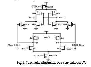
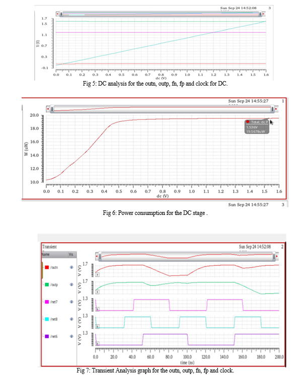
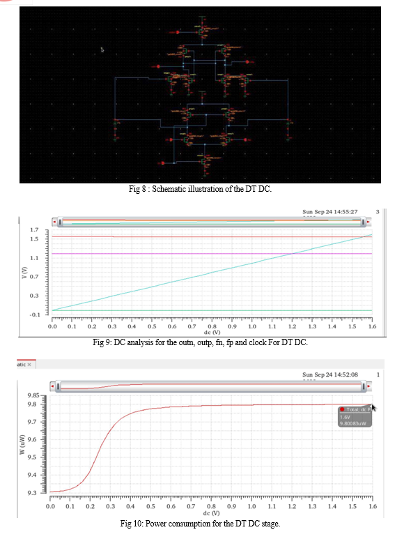
When CLK = 0 and Mtail is turned off, the DC works during the reset phase. To provide the beginning condition and possess a legitimate logical level throughout reset, the reset transistors (M7–M8) pulls both output nodes, Outn and Outp, to VDD. During the comparison phase, Mtail is turned on and transistors M7 and M8 are turned off when CLK is equal to VDD. After being precharged to VDD, output voltages (Outp, Outn) begin to discharge at varying rates according to the matching input voltage (INN/INP).Considering that Outp discharges faster than Outn in the scenario where VINP > VINN, the corresponding pMOS transistor (M5) will turn on to initiate the discharge of Outp (discharged by transistor M2 drain current) when it falls to VDD–|Vthp| before Outn (discharged by transistor M1 drain current). Back-to-back inverters causing latch regeneration (M3, M5 Fig. 2). As a result, Outp releases to the ground and Outn pulls to VDD. The circuits function the opposite way if VINP < VINN.
This is because only the latch's transistors M4 and M3 initially contribute to the positive feedback, which is then amplified by transistors M6 or M5 to initiate full regeneration when the voltage level of 1 output node drops below a threshold. Only slightly is the gate-source voltage of M4 and M3 affected by the voltage drop because the gate-source voltages of transistors M6 and M5 are likewise very small at low supply voltages. Because of the decreased transconductance, this causes the latch 1's delay time to increase. Transistors of DT architecture have two tails. Applications requiring little power use of DT comparator devices. To boost the latch regeneration speed in this technique, raise the voltage differential between the output nodes. During reset phase (CLK = 0, Mtail2, and Mtail1 are off), transistors M3-M4 pre-charge fp and fn nodes to VDD, which consequently results in transistors MR2 and MR1 to discharge the nodes of output to ground.
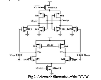
M3–M4 switch off, the voltages at nodes fp and fn begin to decline at a rate determined by IMtail1/Cfn(p) during the decision making phase (CLK = VDD, Mtail1 and Mtail2 turn on), and an input dependent differential voltage Vfn(p) will accumulate atop of this. In addition to providing strong shielding between the I/P and O/P, the stage in between made up of MR1 and MR2 passes Vfn(p) to the cross coupled inverters, lowering the amount of kickback noise. Since the fn and fp nodes in this comparator both discharge to ground, both the stage in between transistors have ultimately cut-off, therefore they are of no use in increasing the latch's effective transconductance. While reset phase, these nodes have to be charged from ground to VDD, power consumption.
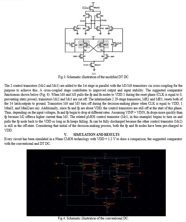
The pros of the previous architecture included high input impedance, rail-to-rail output swing, no static power consumption, and strong resistance to mismatch and noise [1]. As the output nodes' switching speed is not directly impacted by the parasitic capacitances of the input transistors, huge input transistors could be engineered to minimize the offset. However, the disadvantage is that multiple stacked transistors mean that a respectably large voltage supply is necessary to achieve a suitable delay time. This is because, at first, only the latch's transistors M4 and M3 participate in to the positive feedback. However, when voltage level of one output node drops below a threshold, transistors M6 or M5 become active and the full regeneration process begins. The voltage drop has minimal effect on the gate- source voltages of M3 and M4 because the gate-source voltages of transistors M5 and M6 are likewise very small at less supply voltages. As a result, the time delay of the latch increases because the transconductances are reduced. To address the shortcomings of the earlier design, the suggested dynamic DT comparator's schematic diagram is displayed in Fig. 3. The suggested comparator is built using a DT architecture because of its superior performance in low-voltage applications.
Conclusion
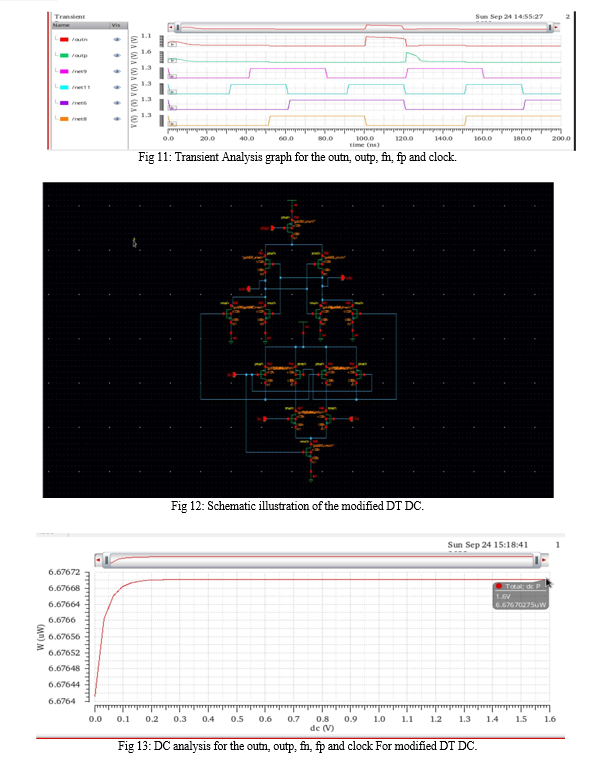
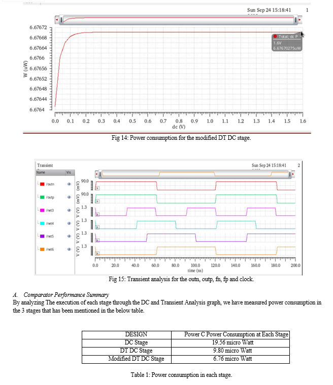
A thorough power evaluations have been instigated for DCs that are timed. There would be a review of two typical structures: conventional DCs and conventional DT DCs. A single rail in a single tail DC is insufficient owing to the huge power supply. Because DT DC provides big output swing and quick operation with minimal power consumption, single tail DCs have smaller output voltage swing. Power is significantly decreased by just supplementing the traditional DT DC combining a few minimum-sized transistors. Previously, in a DT topology, both the fp and fn nodes should be hauled back up again to the VDD each time they discharge to the ground during the decision-making phase of the reset phase. Among the only one of the aforementioned nodes (fp/fn) must be charged during the reset phase of the redesigned comparator, though. This is because less power was needed because, during the previous decision-making stage, one of the nodes had not been discharged depending regarding the status of the control transistors. Comparing this improvement to the traditional DC and DT comparator will likewise yield significant power savings. Additionally, a significant reduction in consumption of power is required for both of the suggested DCs. To enhance comparator performance, a novel DC with lower power and lower voltage capability is built.
References
[1] S. Babayan-Mashhadi and R. Lotfi, \"Analysis and Design of a Low-Voltage Low-Power DoubleTail Comparator,\" in IEEE Transactions on Very Large Scale Integration (VLSI) Systems, vol. 22, no. 2, pp. 343-352, Feb. 2014, doi: 10.1109/TVLSI.2013.2241799. [2] S. S. Chiwande and S. P. Akarte, \"Performance analysis of low voltage, low power dynamic double tail comparator for data convertor application,\" 2016 World Conference on Futuristic Trends in Research and Innovation for Social Welfare (Startup Conclave), Coimbatore, India, 2016, pp. 1-4, doi: 10.1109/STARTUP.2016.7583918. [3] D. Basak, S. M. I. Huq and S. Nath Biswas, \"Design and Analysis of High Speed DC for Area Minimization,\" 2019 2nd International Conference on Innovation in Engineering and Technology (ICIET), Dhaka, Bangladesh, 2019, pp. 1-5, doi:10.1109/ICIET48527.2019.9290619 [4] A. Khorami and M. Sharifkhani, \"A Low-Power High-Speed Comparator for Precise Applications,\" in IEEE Transactions on Very Large Scale Integration (VLSI) Systems, vol. 26, no. 10, pp. 2038-2049, Oct. 2018, doi: 10.1109/TVLSI.2018.2833037.) [5] L. Raju Thoutam, G. Rajya Vardhini, K. Ramya, M. Neeraj, S. Ravikumar and J. Ajayan, \"Design of Low Power 2-Bit Flash ADC using High Performance Dynamic Double Tail Comparator,\" 2022 IEEE Internationa Conference on Nanoelectronics, Nanophotonics, Nanomaterials, Nanobioscience & Nanotechnology (5NANO), Kottayam, India, 2022, pp. 1-5, doi: 10.1109/5NANO53044.2022.9828927. [6] Y. Wang, M. Yao, B. Guo, Z. Wu, W. Fan and J. J. Liou, \"A Low-Power High-Speed DC With a Transconductance-Enhanced Latching Stage,\" in IEEE Access, vol. 7, pp. 93396- 93403, 2019, doi: 10.1109/ACCESS.2019.2927514. [7] Nikoozadeh and B. Murmann, “An analysis of latched comaprator offset due to load capacitor mismatch,” IEEE Trans. Circuits Syst. II, Exp. Briefs, vol. 53, no. 12, pp. 1398–1402, Dec. 2006. [8] J. He, S. Zhan, D. Chen, and R. J. Geiger, “Analyses of static and dynamic random offset voltages in DCs,” IEEE Trans. Circuits Syst. I, Reg. Papers, vol. 56, no. 5, pp. 911–919, May 2009. [9] B. J. Blalock, “Body-driving as a Low-Voltage Analog Design Technique for CMOS technology,” in Proc. IEEE Southwest Symp. Mixed-Signal Design, Feb. 2000, pp. 113–118.
Copyright
Copyright © 2024 Poornima G, Soundarya N. This is an open access article distributed under the Creative Commons Attribution License, which permits unrestricted use, distribution, and reproduction in any medium, provided the original work is properly cited.

Download Paper
Paper Id : IJRASET63031
Publish Date : 2024-05-31
ISSN : 2321-9653
Publisher Name : IJRASET
DOI Link : Click Here
 Submit Paper Online

