Ijraset Journal For Research in Applied Science and Engineering Technology
- Home / Ijraset
- On This Page
- Abstract
- Introduction
- Conclusion
- References
- Copyright
Low-Power Redundant-Transition-Free TSPC DET-FF with STCB for Enhanced Power and Area Efficiency
Authors: K Srikanya
DOI Link: https://doi.org/10.22214/ijraset.2024.65246
Certificate: View Certificate
Abstract
In the contemporary era dominated by graphics processing units (GPUs) and artificial intelligence (AI), flip-flops (FFs) have emerged as power-intensive components within processors. Addressing this power consumption challenge, a pioneering approach introduces a single-phase clock dual-edge-triggering (DET) FF leveraging a single-transistor clocked (STC) buffer (STCB). This STCB employs a singular clocked transistor in the data sampling path, eliminating clock redundant transitions (RTs) and internal RTs observed in alternative DET designs. Validated through post-layout simulations in 22 nm fully depleted silicon on insulator (FD-SOI) CMOS, the proposed STC-DET surpasses existing state-of-the-art low-power DETs in power efficiency, boasting the lowest power-delay-product (PDP) among its counterparts. The modified clock gating, Sapon, Transmission Gate, and gate approach, detailed in the base paper, further refines the TSPC STCDET design, presenting techniques to reduce parameters such as delay or power.
Introduction
I. INTRODUCTION
Especially in light of the pressure from current graphics processing unit (GPU)/artificial intelligence (AI) neural network processors, power consumption has emerged as one of the top problems for CMOS digital designers. Every 3.4 months, the amount of processing power utilized to train AI doubles. In a contemporary processor, the clocking system can use up to 50% of the overall power. Thus, one of the primary elements to resolving the power dissipation issue noted above has been seen as its power optimization.
The two primary components of a processor's clocking system are flip-flops (FFs) and clock distribution networks. Traditional single-phase-clock FFs only process one clock edge at a time to process incoming data, which consumes extra power data processing not yet developed. In order to process data, dual edge-triggering (DET) FFs use both clock edges. This allows them to reduce the clock frequency to half while still retaining the same throughput. A flip-flop is a fundamental building block in digital electronics and computer architecture. It is a sequential logic circuit that can store and transfer binary information. Flip-flops are used to create memory elements, registers, counters, and other sequential logic circuits. A flip-flop operates on clock pulses, which are regular signals that synchronize the operation of digital circuits. The clock signal determines when the flip-flop will store or transfer data. The two most common types of flip-flops are the SR (Set-Reset) flip-flop and the D (Data) flip-flop.
A. SR Flip-Flop
The SR flip-flop has two inputs, the S (Set) input and the R (Reset) input, and two outputs, the Q output and the Q? (complement of Q) output. When the S input is activated, the Q output is set to 1, and when the R input is activated, the Q output is reset to 0. The Q? output is the inverse of the Q output. The SR flip-flop has a potential problem called the "race condition" where both inputs are activated simultaneously, resulting in an undefined state.
B. D Flip-Flop
The D flip-flop has a single input, the D (Data) input, and two outputs, the Q output and the Q? (complement of Q) output. The D input determines the state of the Q output. When the clock signal is triggered, the D input is transferred to the Q output. If the D input is high (1), the Q output becomes high, and if the D input is low (0), the Q output becomes low. The Q? output is the inverse of the Q output.
Flip-flops are widely used in digital systems for data storage, synchronization, and control. By connecting multiple flip-flops together, complex sequential circuits such as registers and counters can be built.
These circuits form the basis for various digital devices and systems, including computers, calculators, and communication devices. Dual-edge and single-edge triggering are concepts related to the behavior of flip-flops and other sequential logic circuits with respect to clock signals.
C. Single-Edge Triggering
Single-edge triggering refers to the condition where the flip-flop changes its state only on a specific edge of the clock signal. The most common type of single-edge triggering is the positive-edge triggering, also known as rising-edge triggering. In positive-edge triggering, the flip-flop samples the input and updates its state only when the clock signal transitions from low to high (rising edge). The flip-flop remains unaffected during the low-to-high transition and holds its previous state until the rising edge occurs. This type of triggering is widely used in most digital systems.
D. Dual-Edge Triggering
Dual-edge triggering, on the other hand, allows the flip-flop to change its state on both edges of the clock signal. It means that the flip-flop can sample the input and update its state when the clock signal transitions from low to high (rising edge) as well as when it transitions from high to low (falling edge). This provides additional flexibility in designing sequential logic circuits. Dual-edge triggering is less common than single-edge triggering and is typically used in specialized applications where specific timing requirements or synchronization needs exist.
The choice between single-edge and dual-edge triggering depends on the design requirements and the specific application. Single-edge triggering is simpler to implement and is sufficient for most digital systems. However, in certain cases, dual-edge triggering may be advantageous, such as when designing high-speed circuits, implementing certain protocols, or achieving precise timing control.
II. EXISTING METHOD
Single-Transition-Capture Double-Edge-Triggered flip-flop is known as STCDET. It is a particular kind of flip-flop design that has a number of benefits over conventional flip-flop designs. Comparing STCDET flip-flops to single-edge-triggered flip-flops, higher data transfer rates are possible. For faster and more effective data processing, STCDET flip-flops essentially double the data transfer rate by recording data on both rising and falling clock edges in a single clock cycle.
Flip-flop performance and dependability can be affected by clock skew, which is a fluctuation in the timing of clock signals. Because STCDET flip-flops employ both clock edges to record data, they are less susceptible to clock skew. This lessens the effect of clock skew on the flip-flop's timing needs. Better Noise Immunity: STCDET flip-flops provide better noise resistance. compared to flip-flops that just have one edge trigger. They are less vulnerable to noise and hiccups in the clock signal since they capture data on both clock edges. This improved noise immunity lowers the possibility of inaccurate data acquisition and aids in maintaining data
Comparing STCDET flip-flops to other flip-flop designs, they can achieve lower power usage. They use less power since the active power dissipation is dispersed over a shorter time due to their greater data transfer rate. Additionally, power optimization strategies like clock gating may be made possible by the decreased susceptibility to clock skew, which will result in even more power savings. In comparison to more sophisticated flip-flop designs, timing analysis for STCDET flip-flops can be simpler. Timing restrictions are possible since data is recorded on both clock edges within a single clock cycle.The design process is streamlined, and it becomes easier. This may result in more rapid and effective design iterations. The implementation of single-edge-triggered flip-flops can be made backward compatible with STCDET flip-flops. Without making significant changes or disrupting the overall system design, this enables smooth integration into current digital systems
If D remains at its current value, there would be no redundant transition because it results in no switching.The remaining two STCBs in the bottom FF are constructed using transistors (N5, N9, N10, P9, P10) and (P6, N11, N12, P11, P12). X_n will be D ′′, which is essentially D, when C L K = 1, turning on the timed NMOS N5 in the bottom master latch (see bottom left of Fig. 4). As a result, P10 and N10 work as a virtual inverter, and input D passes to M I D_n in the bottom master latch [see arrow]. in Fig. 5(b)'s right half]; On the other side, when the bottom slave latch's clocked PMOS P6 switches off, the routes connected to P11 and consequently N12 will also be off. It is also important to note that QT is a no floating node because it has another connection in the top FF that is active when C L K = 1, as was previously discussed.
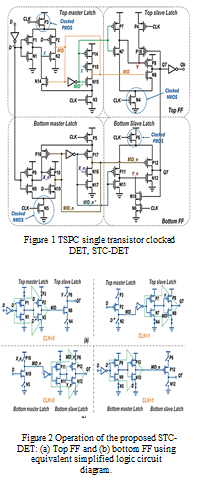
Even if D remains constant, there won't be a redundant transition because it has no impact on QT. STC-DET may sample input at both clock edge positions since the top and bottom slave latches are actuated by positive clock edge and negative clock edge, respectively. Additionally, since the two slave latches are engaged by various clock edges, there The outputs of the slave latches can be coupled together at QT without interference because there is always one latch that is transparent and the other that is opaque for all periods. Furthermore, QT is a perpetually non floating node due to its transparent connection to supply or ground. Additionally, STC-DET can be readily modified to be scannable for supporting the design for test (DFT) by adding an enable signal and scan input to the master latches on the left side. Additionally, it can be changed into a single-edge FF design by including keepers at the top or bottom FF, respectively.
III. PROPOSED METHOD
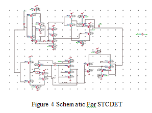
Within CMOS circuits, the scaling of threshold voltage to achieve voltage reduction inherently amplifies subthreshold leakage current, causing a surge in static power dissipation. To counter this challenge, we present an innovative approach encompassing SAPON and Modified Clock Gating techniques for CMOS gate design, effectively curbing leakage current without amplifying dynamic power dissipation. In the SAPON technique, we introduce two leakage control transistors (p-type and n-type) within the logic gate. Crucially, the gate terminal of each leakage control transistor (LCT) is intricately linked to the source of the other, ensuring that one LCT is consistently "near its cutoff voltage" for any input combination. This strategic arrangement substantially elevates the resistance along the path from V/sub dd/ to ground, leading to a noteworthy reduction in leakage currents. The implementation process involves converting the gate-level netlist of the circuit into a static CMOS complex gate, followed by the introduction of LCTs to establish a leakage-controlled circuit. A notable feature of SAPON and Modified Clock Gating lies in their effectiveness during both active and idle states of the circuit, yielding superior leakage reduction when compared to alternative techniques.
In CMOS circuits, the reduction of threshold voltage through voltage scaling induces an escalation in subthreshold leakage current, culminating in elevated static power dissipation. Our novel methodology, denoted as SAPON (Subthreshold Leakage Attenuation through P- and N-type transistors) and Modified Clock Gating, pioneers an effective means of crafting CMOS gates that substantially mitigate leakage current without augmenting dynamic power dissipation. The essence of SAPON involves the incorporation of two leakage control transistors (one p-type and one n-type) within the logic gate. Importantly, the gate terminal of each leakage control transistor (LCT) is intricately linked to the source of the other, ensuring that one LCT consistently hovers "near its cutoff voltage" for any input combination. Consequently, this arrangement elevates the resistance along the path from V/sub dd/ to ground, resulting in a noteworthy reduction in leakage currents. The implementation process entails transforming the gate-level netlist of the specified circuit into a static CMOS complex gate, followed by the introduction of LCTs to establish a leakage-controlled circuit. A notable feature of SAPON is its efficacy in both active and idle states of the circuit, outperforming alternative techniques in leakage reduction.
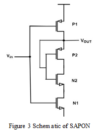
A. Operation of the Top FF in STC-DET
when C L K = 0, and transistors (P2, N2) become equivalent to a virtual inverter [A simplified logic diagram is shown in Fig. 5(a)]. When C L K = 0, the top master latch's clocked PMOS P3 turns on, changing node X to D ′′. In contrast, in the top slave latch in Fig. 4, clocked NMOS N4 is off because C L K = 0, therefore node Y will not be 0, thus PMOS P8 is off. The input then travels to M I D in the top master latch (see arrow in the upper left of the previous picture). VDD and QT cannot connect or GND, which denotes that the top FF's QT is floating (see the top left of Fig. 5(a)).
A negative-triggered STCB is constructed in Fig. 4 by transistors N1, N2, P1, P2, and P3, with the sole timed transistor P3 serving as the signal sampling channel. In contrast to FN_C DET and FS-TSPC (Fig. 3), STCDET does not have the RT that exists between a clocking PMOS and a clocking NMOS. No argument exists either.
A second clock-driven NMOS transistor, N3, is present in the top master latch (top left of Fig. 4), although it is employed in the keeper rather than the data sampling path. It is clocked similarly to transistor P3. The four transistors that are clocking together are all on the data sampling path have been marked out with an arrow in Fig. 4 (P3, N4, N5, and P6). Transistors (N4, N7, N8, P7, P8) build another positive triggered STCB in the top FF.
When C L K = 1, the routes connected to P1 and consequently N2 in the top master latch of Fig. 4 are off because clocked PMOS P3 is off because C L K = 1. The logic state of M I D is therefore maintained by keeper (N3, N15, P14, P15). X will be maintained by pull down keeper (N14, N3) while its logic state is 0. The timed NMOS, N4, however, turns on at the top slave latch, making Y be M I D′′, which is virtually M I D. The signal from M I D, which is just before the clock rising edge, travels to QT as a result of transistors (N8, P8) acting as a virtual inverter. as a result, the top FF is activated at the clock positive edge.
B. Operation of the Bottom FF in STC-DET
The clock NMOS, N5, in the bottom master latch goes off when C L K = 0 in the bottom FF (see bottom left of Fig. 4).As a result, the routes connected to N9 and P10 are inactive, and keeper (N16, N17, P5, P17) maintains the logic state of M I D_n. If the logic state of X_n is 1, keeper (P16, P5) will maintain that state. However, in the bottom slave latch (bottom right of Fig. 4), when C L K = 0, the timed PMOS P6 in the top of the figure switches on, transforming Y _n into M I D_n ′′, which is essentially M I D_n. As a result, P12 and N12 work as a virtual inverter, and the signal of M I D_n appears. I D_n, just before the clock falling edge passes to QT (see arrow in left half of Fig. 5(b)1), is at this time. As a result, on the clock's negative edge, the bottom FF is engaged.
IV. RESULTS
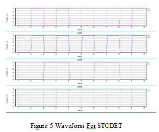
A. Schematic
B. Waveform
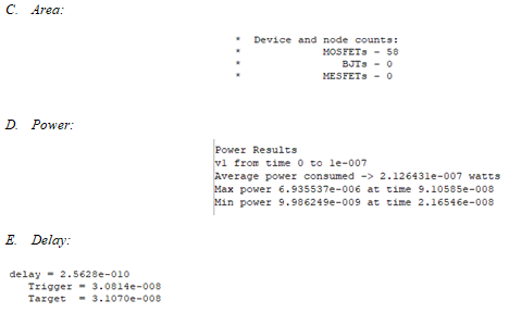
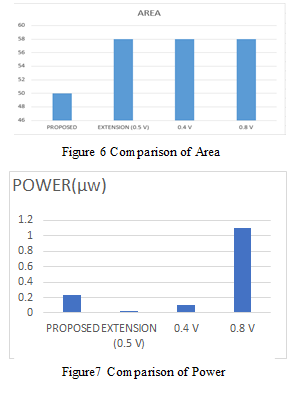
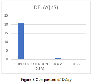
Comparison Table:
|
|
AREA |
POWER |
DELAY |
|
Existing (0.8V) |
50 |
1.164889e-005w |
2.0727e-008ns |
|
Proposed (0.5 V) |
58 |
2.126431e-007w |
2.5628e-010ns |
Conclusion
Introducing a novel and power-efficient design, we propose a distinctive low-power redundant-transition-free dual-edge-triggered flip-flop (DET) referred to as STC-DET. This innovative design leverages Single-Transistor-Clocked (STC) buffers to effectively eliminate redundant transitions (RT) in dual-edge-triggered flip-flops. The positive-triggered and negative-triggered STC buffers within the topology each incorporate only one timed transistor in the data sampling circuit. This configuration eradicates all clock redundant components, transitions, and internal redundant transitions that were present in previous DET systems employing two clocked transistors. Notably, the STC-DET, in addition to being RT-free, exhibits no controversy in terms of power dissipation. Furthermore, in a comprehensive evaluation across various process corners and voltage scenarios for switching activity, the proposed STC-DET outperforms all DET designs by consuming the least amount of power. In conclusion, within the state-of-the-art DET flip-flops, the suggested STC-DET stands out with the lowest power consumption in the average switching activity range..
References
[1] S. Lapshev and S. M. R. Hasan, “New low glitch and low power DET flip-flops using multiple C-elements,” IEEE Trans. Circuits Syst. I, Reg. Papers, vol. 63, no. 10, pp. 1673–1681, Oct. 2016. [2] J. Tschanz, S. Narendra, Z. Chen, S. Borkar, M. Sachdev, and V. De, “Comparative delay and energy of single edge-triggered and dual edgetriggered pulsed flip-flops for high-performance microprocessors,” in Proc. ISLPED, 2001, pp. 147–152 [3] A. Karimi, A. Rezai, and M. M. Hajhashemkhani, “A novel design for ultra-low power pulse-triggered D-flip-flop with optimized leakage power,” Integration, vol. 60, pp. 160–166, Jan. 2018. [4] Lee, G. Shin, and Y. Lee, “A fully static true-single-phaseclocked dual-edge-triggered flip-flop for near-threshold voltage operation in IoT applications,” IEEE Access, vol. 8, pp. 40232–40245, 2020. [5] R. Hossain, L. D. Wronski, and A. Albicki, “Low power design using double edge triggered flip-flops,” IEEE Trans. Very Large Scale Integr. (VLSI) Syst., vol. 2, no. 2, pp. 261–265, Jun. 1994. [6] H. You, J. Yuan, Z. Yu, and S. Qiao, “Low-power retentive true single-phase-clocked flip-flop with redundant-precharge-free operation,” IEEE Trans. Very Large Scale Integr. (VLSI) Syst., vol. 29, no. 5, pp. 1022–1032, May 2021. [7] P. . Zhao et al., “Low-power clocked-pseudo-NMOS flip-flop for level conversion in dual supply systems,” IEEE Trans. Very Large Scale Integr. (VLSI) Syst., vol. 17, no. 9, pp. 1196–1202, Sep. 2009. [8] A. Bonetti, A. Teman, and A. Burg, “An overlap-contention free truesingle-phase clock dual-edge-triggered flip-flop,” in Proc. IEEE Int. Symp. Circuits Syst. (ISCAS), May 2015, pp. 1850–1853. [9] M. W. Phyu, K. Fu, W. L. Goh, and K. S. Yeo, “Power-efficient explicit-pulsed dual-edge triggered sense-amplifier flip-flops,” IEEE Trans. Very Large Scale Integr. (VLSI) Syst., vol. 19, no. 1, pp. 1–9, Jan. 2011.
Copyright
Copyright © 2024 K Srikanya. This is an open access article distributed under the Creative Commons Attribution License, which permits unrestricted use, distribution, and reproduction in any medium, provided the original work is properly cited.

Download Paper
Paper Id : IJRASET65246
Publish Date : 2024-11-14
ISSN : 2321-9653
Publisher Name : IJRASET
DOI Link : Click Here
 Submit Paper Online

