Ijraset Journal For Research in Applied Science and Engineering Technology
- Home / Ijraset
- On This Page
- Abstract
- Introduction
- Conclusion
- References
- Copyright
Low-Power Retentive True Single Phase Clocked (TSPC) D-Flip-Flop with Redundant Precharge Free Operation
Authors: Levaku Jhansi, Y. Suneel Kumar, R L B R Prasad Reddy
DOI Link: https://doi.org/10.22214/ijraset.2024.64149
Certificate: View Certificate
Abstract
In this paper, optimizing power consumption of flip-flops (FFs) can significantly reduce the power of digital systems. In this article, an energy-efficient retentive true single- phase-clocked (TSPC) FF is proposed. With the employment of input-aware precharge scheme, the proposed TSPC FF precharges only when necessary. In addition, floating node analysis and transistor level optimization are employed to further ensure the high energy efficiency of the FF without significantly increasing the area. As The proposed Low power Retentive TSPC FF consumes less power which can be used in application like PLL (phased Lock loop )The main objective of a PLL is to generate a signal in which the phase is the same as the phase of a reference signal. The main Block For this is To design Phase frequency Circuit, Which is designed by using Low power Retentive TSPC FF To Give the better Results compare to conventional Circuit with a power Supply of 1.2 V by using Tanner EDA Tool.
Introduction
I. INTRODUCTION
Flip-flops are the basic building block of the data path structure. They allow for the storage of data, processed by combinational circuit and synchronization of operation at a given clock frequency. They are the fundamental building block of the digital electronics systems used in computers and many other types of systems. Flip flop can be either simple or clocked; simple devices are known as latches. A latch is level sensitive, and mainly used as storage element. And clocked devices are known as flipflop.
Flip-flop is edge sensitive means their output only changes on a single type of clock edge (positive or negative going edge). Flip-Flop is an electronic circuit that stores the logical state of one or more data input signal in response to a clocking pulse. They are often used in computational circuits to operate in selected sequences during recurring clock intervals to receive and maintain data for a limited time period sufficient for other circuits within a system to further process data [1].
Data is stored in flip-flop at each rising and falling edge of clock signal so that it can be applied as inputs to other combinational or sequential circuits, such flip-flops that store data on rising or falling edge of clock are referred as single edge triggered flip flops and the flip-flops that store data on both the rising and falling edge of a clock pulse are referred as double edge triggered flip-flops.
In CMOS circuit there are 3 sources of power dissipation, first static (leakage) power dissipation which is related to the logical states of the circuits and independent of switching activity. Second is short circuit power dissipation when both NMOS and PMOS transistor in the circuit is turned on simultaneously for short duration of time during switching. And as a result direct current path between powers supply and ground is formed.
And third is Dynamic (switching) power dissipation which is caused by power dissipation during switching activity [4]. Another important timing value for a flip-flop is the clock-to-output delay (tP) i.e. the time taken by a flip-flop to change its output after the clock edge. In digital electronics, the power-delay product which is also known as switching energy, is FOM (figure of merit) correlated with the energy efficiency of a logic gate.
Power delay product is used to evaluate the performance of CMOS process. When the technology scales down, total power dissipation decreases and at the same time delay varies depends upon supply voltage, threshold voltage, aspect ratio, oxide thickness, and load capacitance [5].
II. RELATED WORK
A. Low power flip-flop designs featuring efficient embedded logic
A DML mode logic is introduced here which improves the speed performance of the design, also achieving significant energy consumption reduction. The large capacitance in precharge node is eliminated by the DDFF and DDFF-ELM designs by following a split dynamic node structure. The DDFF offers power reduction. The DDFF-ELM reduces pipeline overhead. 4-b Johnson up-down counter is used to magnify the performance improvement of the designs, to which the DML logic is introduced. An area, power, and speed efficient method is presented here that incorporates complex logic functions into the flip-flop. The DML logic used in DDFF-ELM helps to achieve low power and high speed requirements.
B. Designing and Evaluating Redundancy-Based Soft-Error Masking on a Continuum of Energy versus Robustness
Near-threshold computing is an effective strategy to reduce the power dissipation of deeply-scaled CMOS logic circuits. However, near-threshold strategies exacerbate the impact of delay variations on device performance and increase the susceptibility to soft errors due to narrow voltage margins. The objective of this work is to develop and assess design approaches that leverage tradeoffs between performance and the resilience of fault masking coverage for various soft-error mitigation techniques. The primary insight from this work is identification of redundancy-based hardening techniques that can deliver increased benefits in terms of the fault coverage energy ratio (FCER) for the leveraged tradeoffs within iso-energy constraints at near-threshold voltage (NTV). Simulation results demonstrate that temporal redundancy approaches offer favorabletradeoffs in terms of FCER. They exhibit reduced impact on performance variations and achieve extensive soft fault masking, therefore improving the system robustness within acceptable delay constraints. Meanwhile, it is shown that a hybrid redundancy approach can be used to protect a low-power system to maintain throughput while tolerating soft errors. We demonstrate how the FCER metric can be used as an optimization parameter to guide circuit synthesis to meet performance and robustness goals. Finally, the impact of design diversity on spatial and hybrid redundancy at NTV is assessed in terms of FCER and delay variation to form overall recommendations regarding soft-error mitigation at NTV.
III. EXISITING SYSTEM
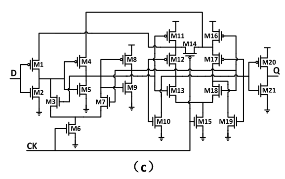
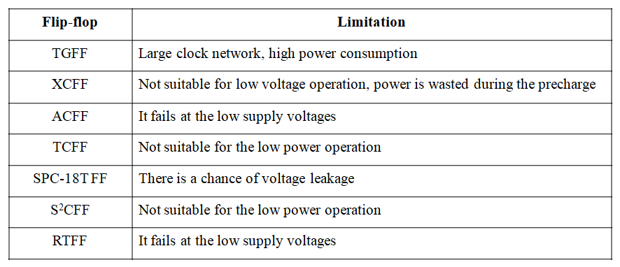
In existing system, several state-of-the-art low-power FFs are reviewed and the limitations are analyzed. All the listed FFs are single-phase-clocked FFs, which optimize the number of transistors related to the clock signal compared to TGFF.
In [13], a cross-charge control FF (XCFF) is proposed to reduce charged gate capacitance so as to reduce power consumption. As shown in Figures there is strong current contention at the output node of XCFF, so XCFF is not suitable for low voltage operation. Furthermore, XCFF needs to precharge some internal nodes no matter what the input data is, and extra power is wasted during the precharge and discharge operation.
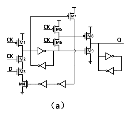
Figure – 1: XCFF
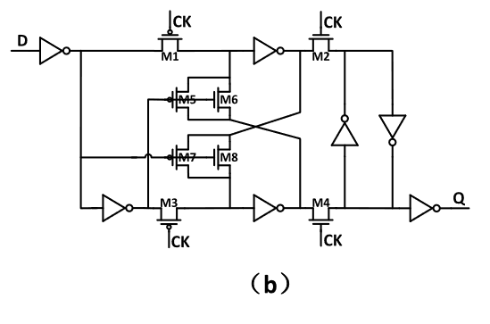
Figure – 2: ACFF
Figure – 3: TCFF
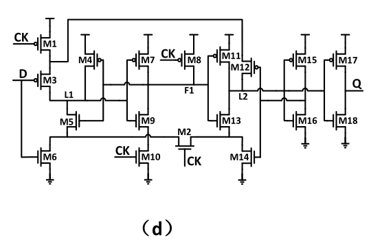
Figure – 4: SPC-18T
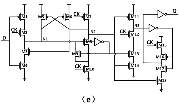
Figure – 5: S2CFF
Table – 1: Existing System Limitations
IV. PROPOSED SYSTEM
In the proposed system, the structure of the proposed FF is described in detail. In order to minimize the power consumption of FF, any unnecessary transitions of internal nodes should be removed. We start with S2CFF which is retentive TSPC and suitable for low voltage operations. To eliminate the redundant precharge and discharge operations, the FF is optimized by following steps. Firstly, unnecessary precharge operation of the internal node N2 is totally removed by the input-aware precharge scheme. Secondly, the floating node is under consideration to avoid short current which would greatly increase power consumption. Finally, unnecessary transistors are merged or removed to decrease the area.
Since the voltage of floating nodes may change after transition due to the leakage current, it is necessary to carefully analyze floating nodes to avoid the generation of short-circuit paths. With the insertion of the input-aware transistor, the voltage of the node N2 is no longer precharged to VDD at the negative half cycle of CK when the input is 0.
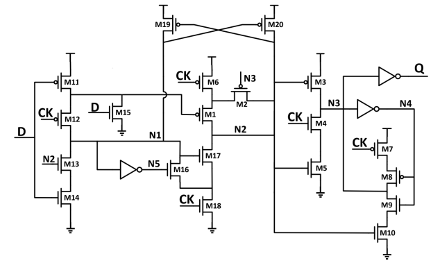
Figure-6: Schematic of the proposed System
When the output Q = 1, which means N3 = 0, the state of N3 is maintained by M9 and M10. To keep the transistor M3 OFF and the transistor M10 ON at that time, the voltage of N2 needs to keep high. In order to avoid N2 becoming floating while the next input data is 0, a transistor M2 is inserted to keep the voltage of N2. M2 is controlled by N3 and provides a precharge path for N2 when q = 1.
When the output Q = 0, N3 = 1, the state of N3 is maintained by M7 and M8. If the precharge path of N2 is cutoff at that time, which means the input data is 0 and the voltage of N2 does not charge to high when CK is low, the only effect is that M3 is ON, which will not lead to a short circuit path. When N3 = 1, CK = 0, and D = 0, the node N3 is isolated from its pull-down path (M4 and M5) through M4 (CK = 0), so the voltage of N2 has no effect on the node N3. Similarly, N1 is isolated from its pull-down path (M13 and M14) through M14 (D = 0), and the voltage of N2 has no effect on the node N1. Therefore, the floating of the node N2 is negligible in this case.
The function of the FF is correct and the redundant precharge operation is removed after adopting the input-aware precharge scheme and floating node analysis, but the FF can be further improved. The PMOS M11_1 which is used to generate the inversion of the input data can be merged into M11. But the NMOS M15 cannot be merged into M14 at the same time. Once both PMOS and NMOS are merged, which means the drain of M11 and M14 is directly connected, which can lead to functional failures of the FF. Thus, the NMOS M15 is reserved. The transistor M13 in S2CFF is removed because it no longer plays a significant role in the proposed structure.
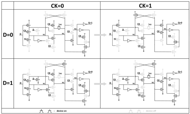
Figure-7: Operation diagram of the proposed FF at different D and CK
- High-to-Low Transition: When CK is low, the node N1 is charged to VDD through M11 and M12, the node N2 is charged to VDD through M6 and M2, the node N3 keeps low through M9 and M10, and the output Q keeps high. At the rising edge of CK, N2 is discharged to GND through M17 and M18, and then M13 is turned off to isolate the FF from changes in the input data. At the same time, the node N3 is charged to VDD through M3, and then the output Q changes to 0. The voltage of N1 keeps high through M19, while the voltage of N2 keeps low through M17 and M18 during the positive half cycle of CK.
- Low-to-High Transition: When CK is low, N2 is charged to VDD through M6 and M1, N1 is discharged to GND through M13 and M14, the node N3 keeps high through M7 and M8, and the output keeps low. At the rising edge of CK, the input data is isolated through M12, and the node N3 is discharged to GND through M4 and M5, then the output Q changes to 1. The voltage of N1 keeps low through M16 and M18, while the voltage of N2 keeps high through M20 during the positive half cycle of CK.
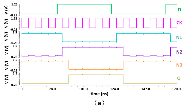
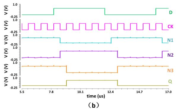
Figure-8: Transient waveform of the proposed FF
A. Algorithm
- Create the project in the S-edit
- Import all the library files.
- Construct the circuit by using the library files.
- And then for that circuit generate the Tspice file.
- Then the code will be generated.
- Then we have to give the input and the operating
- Signals by inserting the code.
- Print the output responses by giving the appropriate commands.
- Execute the code If there is any error check and rectify it and the execute the code.
- The responses will be displayed in the W-edit.
V. RESULTS
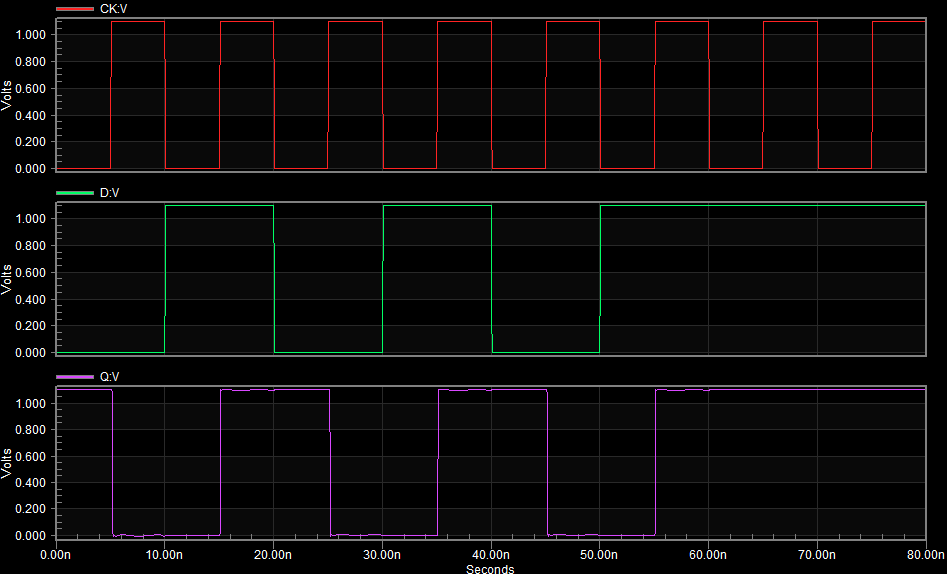
Figure-9: Proposed System outputs
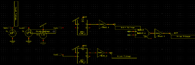
Figure-10: phase detector
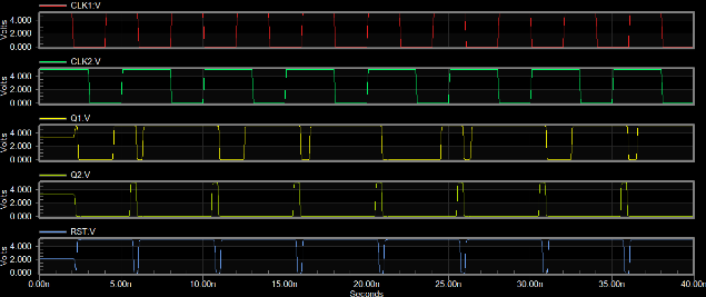
Figure-11: Waveforms
Table – 2: Comparison table of Existing System and Proposed System
Conclusion
By removing the redundant precharge and discharge operations, the power of the proposed flip-flop is greatly reduced and it will avoid the generation of the short-circuit paths.
References
[1] L. Atzori, A. Iera, and G. Morabito, “The Internet of Things: A survey,” Comput. Netw., vol. 54, no. 15, pp. 2787–2805, Oct. 2010. [2] T. Tekeste, H. Saleh, B. Mohammad, A. Khandoker, and M. Ismail, “A nano-watt ECG feature extraction engine in 65-nm technology,” IEEE Trans. Circuits Syst. II, Exp. Briefs, vol. 65, no. 8, pp. 1099–1103, Aug. 2018. [3] T. Tekeste, H. Saleh, B. Mohammad, and M. Ismail, “Ultra-low power QRS detection and ECG compression architecture for IoT healthcare devices,” IEEE Trans. Circuits Syst. I, Reg. Papers, vol. 66, no. 2, pp. 669–679, Feb. 2019. [4] A. Pullini, D. Rossi, I. Loi, G. Tagliavini, and L. Benini, “Mr. Wolf: An energy-precision scalable parallel ultra low power SoC for IoT edge processing,” IEEE J. Solid-State Circuits, vol. 54, no. 7, pp. 1970–1981, Jul. 2019. [5] J. P. Cerqueira, T. J. Repetti, Y. Pu, S. Priyadarshi, M. A. Kim, and M. Seok, “Catena: A near-threshold, sub-0.4-mW, 16-core programmable spatial array accelerator for the ultralow-power mobile and embedded Internet of Things,” IEEE J. Solid-State Circuits, vol. 55, no. 8, pp. 2270–2284, Aug. 2020. [6] J. L. Shin et al., “The next generation 64b SPARC core in a T4 SoC processor,” IEEE J. Solid-State Circuits, vol. 48, no. 1, pp. 82–90, Jan. 2013. [7] L. Moreau, R. Dekimpe, and D. Bol, “A 0.4 V 0.5fJ/cycle TSPC flipflop in 65 nm LP CMOS with retention mode controlled by clockgating cells,” in Proc. IEEE Int. Symp. Circuits Syst. (ISCAS), May 2019, pp. 1–4. [8] A. Andrei, P. Eles, O. Jovanovic, M. Schmitz, J. Ogniewski, and Z. Peng, “Quasi-static voltage scaling for energy minimization with time constraints,” IEEE Trans. Very Large Scale Integr. (VLSI) Syst., vol. 19, no. 1, pp. 10–23, Jan. 2011. [9] X. Zhang et al., “32bit×32bit multiprecision razor-based dynamic voltage scaling multiplier with operands scheduler,” IEEE Trans. Very Large Scale Integr. (VLSI) Syst., vol. 22, no. 4, pp. 759–770, Apr. 2014. [10] W.-J. Tsou et al., “Digital low-dropout regulator with anti PVT-variation technique for dynamic voltage scaling and adaptive voltage scaling multicore processor,” in IEEE Int. Solid-State Circuits Conf. (ISSCC) Dig. Tech. Papers, Feb. 2017, pp. 338–339. [11] S. Jain, L. Lin, and M. Alioto, “Dynamically adaptable pipeline for energy-efficient microarchitectures under wide voltage scaling,” IEEE J. Solid-State Circuits, vol. 53, no. 2, pp. 632–641, Feb. 2018. [12] J. Lee et al., “A self-tuning IoT processor using leakage-ratio measurement for energy-optimal operation,” IEEE J. Solid-State Circuits, vol. 55, no. 1, pp. 87–97, Jan. 2020. [13] A. Hirata, K. Nakanishi, M. Nozoe, and A. Miyoshi, “The cross chargecontrol flip-flop: A low-power and high-speed flip-flop suitable for mobile application SoCs,” in Dig. Tech. Papers. Symp. VLSI Circuits, Jun. 2005, pp. 306–307. [14] C. K. Teh, T. Fujita, H. Hara, and M. Hamada, “A 77% energy-saving 22-transistor single-phase-clocking D-flip-flop with adaptive-coupling configuration in 40 nm CMOS,” in IEEE Int. Solid-State Circuits Conf. (ISSCC) Dig. Tech. Papers, Feb. 2011, pp. 338–339. [15] N. Kawai et al., “A fully static topologically-compressed 21-transistor flip-flop with 75% power saving,” IEEE J. Solid-State Circuits, vol. 49, no. 11, pp. 2526–2533, Nov. 2014. [16] Y. Cai, A. Savanth, P. Prabhat, J. Myers, A. S. Weddell, and T. J. Kazmierski, “Ultra-low power 18-transistor fully static contentionfree single-phase clocked flip-flop in 65-nm CMOS,” IEEE J. Solid-State Circuits, vol. 54, no. 2, pp. 550–559, Feb. 2019. [17] Y. Kim et al., “A static contention-free single-phase-clocked 24T flip flop in 45 nm for low-power applications,” in IEEE Int. Solid-State Circuits Conf. (ISSCC) Dig. Tech. Papers, Feb. 2014, pp. 466–467. [18] F. Stas and D. Bol, “A 0.4-V 0.66-fJ/cycle retentive true-single-phaseclock 18T flip-flop in 28-nm fully-depleted SOI CMOS,” IEEE Trans. Circuits Syst. I, Reg. Papers, vol. 65, no. 3, pp. 935–945, Mar. 2018. [19] F. S. Alghareb, R. A. Ashraf, and R. F. DeMara, “Designing and evaluating redundancy-based soft-error masking on a continuum of energy versus robustness,” IEEE Trans. Sustain. Comput., vol. 3, no. 3, pp. 139–152, Jul. 2018. [20] P. E. Dodd, M. R. Shaneyfelt, J. R. Schwank, and J. A. Felix, “Current and future challenges in radiation effects on CMOS electronics,” IEEE Trans. Nucl. Sci., vol. 57, no. 4, pp. 1747–1763, Aug. 2010. [21] M. Fazeli, A. Patooghy, S. G. Miremadi, and A. Ejlali, “Feedback redundancy: A power efficient SEU-tolerant latch design for deep sub-micron technologies,” in Proc. 37th Annu. IEEE/IFIP Int. Conf. Dependable Syst. Netw. (DSN), Jun. 2007, pp. 276–285. [22] Z. Huang, “A high performance SEU-tolerant latch for nanoscale CMOS technology,” in Proc. Design, Automat. Test Eur. Conf. Exhib. (DATE), 2014, pp. 1–5.
Copyright
Copyright © 2024 Levaku Jhansi, Y. Suneel Kumar, R L B R Prasad Reddy. This is an open access article distributed under the Creative Commons Attribution License, which permits unrestricted use, distribution, and reproduction in any medium, provided the original work is properly cited.

Download Paper
Paper Id : IJRASET64149
Publish Date : 2024-09-03
ISSN : 2321-9653
Publisher Name : IJRASET
DOI Link : Click Here
 Submit Paper Online


