

Ijraset Journal For Research in Applied Science and Engineering Technology
Microstrip Antenna for Wideband Application using Inset Feeding
Authors: Dr. Jagadeesha S, Dr. Prathibha Kiran, Syed Yousuff Masood, Mohammed Fuzail , Kushal T K , Ningappa T Pujar
DOI Link: https://doi.org/10.22214/ijraset.2024.66016
Certificate: View Certificate
Abstract
This paper presents the design and implementation of a microstrip antenna array optimized for wireless communication. The proposed design focuses on enhancing gain, bandwidth, and compactness, and efficient feeding techniques. Simulation using IE3D software validated the design, achieving a gain of 3.17 db with a return loss of - 46.93db for the 4-elemental array. Practical testing with a Vector Network Analyzer confirmed its applicability for technologies like 5G and Wi-Fi. The results demonstrate a high-performance, cost-effective solution for modern wireless system
Introduction
I. INTRODUCTION
The rapid growth of wireless communication has driven the demand for efficient and compact antenna designs. Microstrip antennas, with their lightweight and low-profile features, are increasingly popular for applications like 5G, Wi-Fi, and IoT. However, challenges such as limited bandwidth and mutual coupling remain significant.
This paper addresses these issues by designing a microstrip antenna array and advanced feeding technique. Key contributions include optimizing gain and bandwidth while ensuring compactness and compatibility with modern wireless systems.
II. METHODOLOGY
A. Design Overview
The antenna consists of a rectangular microstrip patch on an FR4 substrate (, thickness = 1.6 mm). The array configurations include 1, 2, and 4 elements arranged linearly for enhanced directivity and gain.
Elemental Width:
The following dimensions have to be determined:
- Width of the Patch (W).
- Length (L).
- Width (Wo) of 5002 microstrip transmission line (feed-line).
- Inset distance (yo) for the feed-line for 50SQ impedance matching
B. Design Procedure
- For an efficient radiator, a practical width that leads to good radiation efficiencies is given as,
W = 
 ----------------(1)
Where, c =3 X 10⁸ m/s is the free-space velocity of light.
W=38.036 mm
- The effective dielectric constant (&) of the microstrip antenna can be calculated using equation given below,
 e =
e = 
 -----(2)
 e=4.0858
- Once W is found using step 1 the extension of the length AL can be determined using AL equation [3.2] given below,
 = 0.412 [
  ]—(3)
]—(3)
- The actual length of the patch can be found by solving for L using equation,
L= 
L=29.44mm. ---------(4)
- The resonant input conductance (G) of the one slot of the patch can found using equation given bellow:
G= w/120 0[1-1/24(k0 h)2]
G -2.534X 10⁻³ seimens
Where ko is the free-space wave number given by,
K0=211/A0
K0= 50.26
The resonant input resistance of the patch can be can be determined approximately using equation given as,
Rin (y=0) 1/2G1
=197.316 ------(5)
- Given the resonant input resistance, the inset distance (yo) for matching the input resistance to 502 can be calculated using equation as follows,
Rin (y-y0) = Rin(y=0cos2(II/Ly0)
y0 = 9.77mm ---------(6)
- The actual resonant frequency of the patch approaches the value for ideal case (infinite ground plane) when increase in size (d) is o20 on all sides of the patch metallization.
d= 0/20
d =6.25 ---------(7)
To be on the safer side we decided to keep d=30mm since as the ground plane size increases the size of the back lobe reduces.
- The microstrip transmission line for the patch can be designed for 500 characteristic impedances using,
Where,
Wo= width of the transmission line
h= thickness of the substrate
Step 1: Calculation of Effective dielectric constant (Eref):
The effective dielectric constant is:
reff =  1/2
1/2
Substituting, r =2.45, W=47.5 mm and h=1.58 mm
we get:
reff = 2.3368---------(8)
Step 2: Calculation of the Effective length ( Leff):
The effective length is:
Leff = 
Substituting Ereff =2.3368, c =3.00e+008 m/s and f=2.4 GHz
we get: L=0.0406 m =36.625 ---------(9)
Step 3: Calculation of the length extension (DL):
The length extension is:
DL = 0.412h 
Substituting E=2.3668, W= 47.5 mm and h= 1.58 mm
we get: AL=0.81 mm ---------(10)
Step 4: Calculation of actual length of patch (L):
The actual length is obtained by:
L= Leff -2DL
Substituting Leff = 40.625 mm and DL 0.81 mm
we get: L=39 m=39 nm
and A=Z0/60( r+1/2)1/2+(( r+1/ r-1) (0.23+0.11/ r)
A=1.3459 ---------(11)
Then,
W0/h =(8e15294/e2*1.5294-2)
W0=2.4088mm (for h=1.6mm)
Calculations for 2 Elements
Width of Feedline- 40.35-31.55
=8.8
Length of Feedline- 24.0044-1.2044
Length 24.0044-1.2044
= 22.8
Spacing-86.62-14.72
= 71.9
Calculations for 4 Elements
Width of Feedline- 25.27-22.45
=2.82
Length of Feedline- 57.13-40.33
= 16.8
X Co-ordinate Spacing- 66.73-19.01
=47.72
Y Co-ordinate Spacing- 57.18+14.72
=71.9
Table 1 Measurements of Length and Width of Ground Planes
|
No. of Element |
Ground plane Length Lg(mm) |
Ground plane Width Wg(mm) |
|
Single Element |
50mm |
40mm |
|
2 Element |
70mm |
140mm |
|
4 Element |
85mm |
295mm |
C. Design Implementation
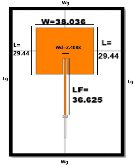
Figure 1 Simulated 1 Elemental array Antenna
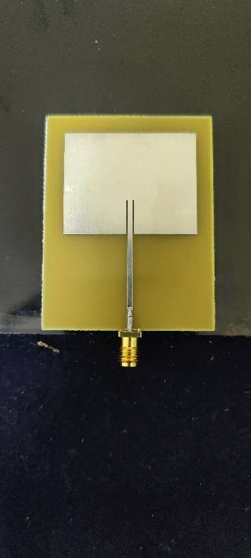
Figure 2 Fabricated 1Elemental array Antenna
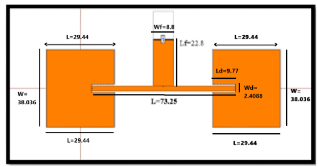
Figure 3 Simulated 2 Element Antenna
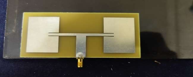
Figure 4 Fabricated 2 Element Antenna
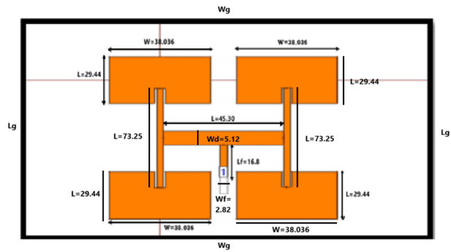
Figure 5 Simulated 4Element Antenna
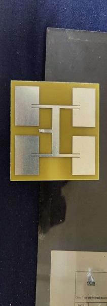
Figure 6 Fabricated 4Element Antenna
D. Software Requirements
IE3D: 1E3D is a powerful electromagnetic simulation software widely used in the field of antenna design, microwave circuits, and electromagnetic compatibility analysis. Developed by Ze land Software Inc., IE3D offers advanced computational capabilities, enabling engineers and researchers to accurately model, simulate, and optimize complex electromagnetic structures. This comprehensive analysis aims to delve into the key features, capabilities, and applications of IE3D, highlighting its strengths and limitations within the realm of electromagnetic simulations.
E. Hardware Requirement
Vector Network Analyser: Vector Network Analysers (VNA) are essential electronic test instruments used in the field of radio frequency (RF) and microwave engineering. They play a crucial role in characterizing and analysing the performance of various RF and microwave devices, such as filters, amplifiers, antennas, and transmission lines. VNAs provide precise measurements of complex impedance, scattering parameters (S-parameters), and other electrical properties, enabling engineers and researchers to optimize the design, development, and troubleshooting of high-frequency circuits. The VNA works by transmitting a known signal into the DUT and then measuring the amplitude and phase of the resulting signal at the input and output ports of the device. By analysing these measurements, the VNA can determine the characteristics of the DUT.
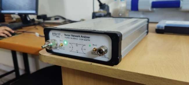
Figure 7 Vector Network Analyse
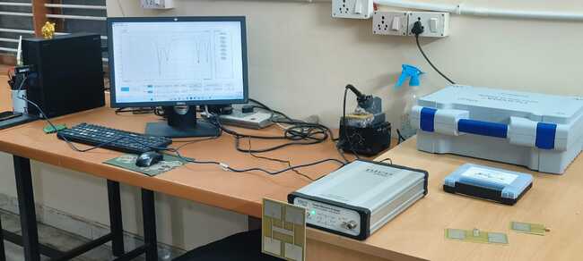
Taking readings of antenna with help of VNA
III. FABRICATION PROCESS:
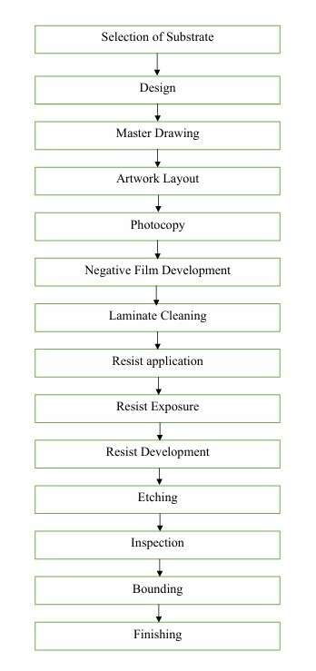
Figure 8 Flow chart of Fabrication process
Microstrip antenna fabrication requires meticulous attention to detail to maintain high dimensional tolerances and avoid bandwidth reduction. The process involves generating artwork from a drawing, ensuring accuracy up to four decimal points. The artwork is prepared on stabline, Rubylith film, or buffer paper, and the dimensions are verified using precision cutting and optical scanning. A high-resolution negative is produced for exposing the photoresist, which is applied to the laminate. After proper adhesion, the laminate is exposed to light, polymerizing the exposed photoresist. The developed antenna is then etched, followed by removal of the photoresist. Visual and optical inspection ensures dimensional accuracy and performance. Smooth edges are achieved, and if desired, a thermal cover bonding may be applied. The final assembly is cooled, inspected, and prepared for further use The above procedure comprises the general steps necessary in producing a microstrip antenna. The substances used for the various processes e. g., cleaning, etching or the tools used for machining etc depends on the substrate chosen.
IV. RESULTS & DISCUSSION
A. Simulated Results
1) Single Element
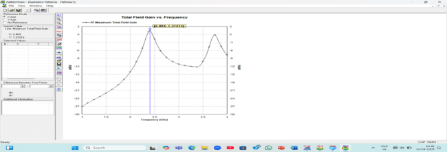
Figure 9 Gain of Single element

Figure 10 Return loss vs Frequency graph of single element
2) Element
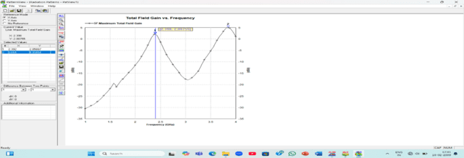
Figure 11 Gain of 2 element
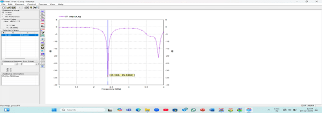
Figure 12 Return loss vs Frequency graph of 2 element
3) Element

Figure 13 Gain of 4 elements
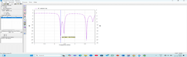
Figure 14 Return loss vs Frequency graph of 4 elements
B. Practical Result
1) Single Element
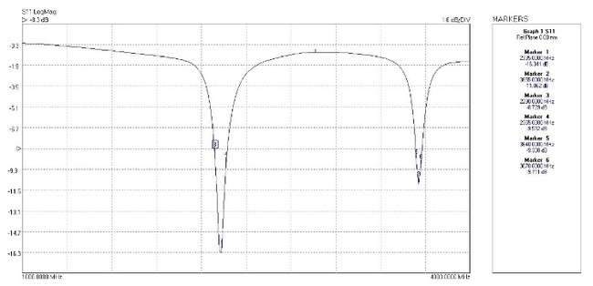
Figure 15 Practical Return loss vs Frequency of Single element
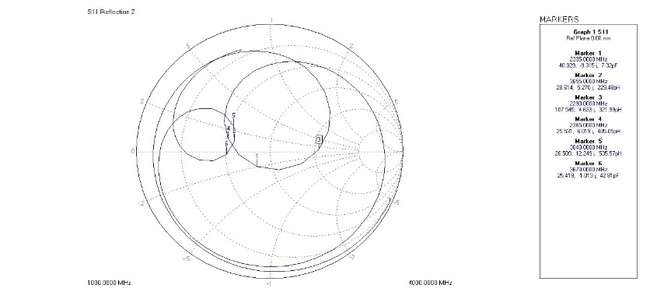
Figure 16 Smith chart of Single element
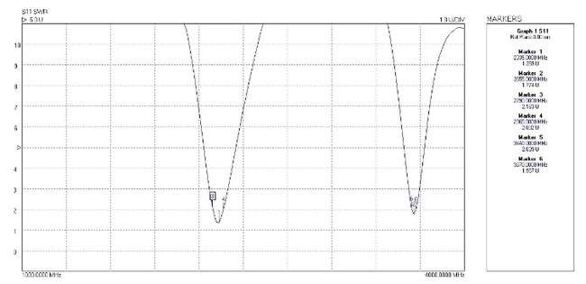
Figure 17 VSWR
2) Element
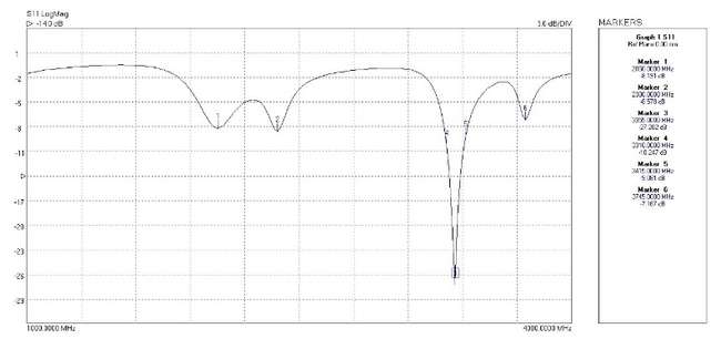
Figure 18 Practical Return loss vs Frequency of 2 Element
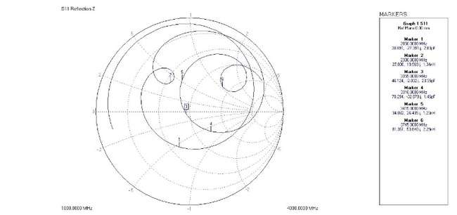
Figure 19 Smith chart of 2 element

Figure 20 VSWR
3) Element
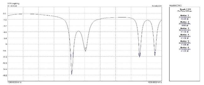
Figure 21 Practical Return Loss vs Frequency of 4 Element
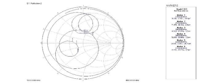
Figure 22 Smith chart of 4 Element
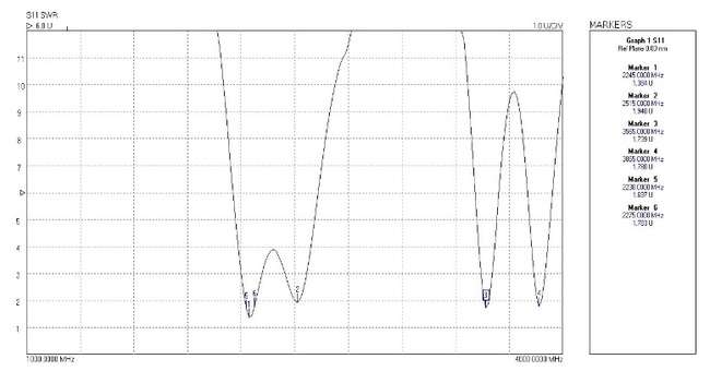
Figure 23 VSWR
Comparison table
|
ELEMENTS |
RESONANT FREQUENCY(GHz) |
GAIN
|
RETURN LOSS (dB) |
||
|
Sim |
Practical |
Sim |
Practical |
||
|
1 ELEMENT |
2.404 |
2.440 |
1.37 |
-14.06 |
-16.341 |
|
2 ELEMENT |
2.398 |
2.357 |
2.08 |
-10.17 |
- 8.191 |
|
4 ELEMENT |
2.302 |
2.322 |
3.02 |
-13.98 |
-15.845 |
Table 1 Comparison Table of without Fractal geometry
Conclusion
Research article Summarizes the effectiveness of a microstrip antenna for wireless communication. The proposed design achieved superior gain bandwidth by using inset feed technique. The prototype design antenna which is designed at 2.4GHz for WIFI application for single element equivalent gain is achieved 1.37. For 2 elemental array antenna incremental change in gain is of 2.08.Similarly for 4 elemental array antenna we have achieved the highest results comparatively with incremental gain of 3.02.
References
[1] U. Keskin, B. Döken and M. Kartal, \"Bandwidth Improvement in Microstrip Patch Antenna\", 2017 8th International Conference on Recent Advances in Space Technologies (RAST), Istanbul, Turkey, pp. 215-219, 2023. [2] Mishra R, Tripathi V S, “A Compact Circular Disc Shaped Monopole Antenna for UWB Applications”, International Journal of Applied FCC, [3] Tomar S. and Kumar A., “Design of a Triple band-notched UWB Planar Monopole Antenna”, Journal of Microwaves, H. D. Chen,“ Broadband CPW-fed square slot antennas with a widened tuning stub,” IEEE Trans. Antennas Propag, vol. 51, pp. 2016-12017August 2018. [4] J. Y. Chiou, J. Y. Sze, and K. L. Wong, “A broad-band CPW - fed strip - loaded square slot antenna,” IEEE Antennas Propag., vol. 51, pp. 719-721, April 2018. [5] W. S. Chen and B. H. Kao, “A Triple-band Polygonal Slot Antenna for WiMAX Applications,” Microwave Journal, vol. 50, p. 134-143, January 2023. [6] J. Y. Jan and J. W. Su, “Bandwidth enhancement of a printed wide-slot antenna with a rotated slot,” IEEE Trans. Antennas Propag,, vol. 53, pp.2111-2114, June 2017. [7] J. Y. Jan and J. C. Kao, “Novel Printed Wide -Band RhombusLike Slot Antenna with an Offset Microstrip-Fed Line,” IEEE Antennas and Wireless Propag. Lett., vol. 6, pp.249-251, 2021. [8] W. S. Chen and F. M. Hsieh, “Broadband design of the printed triangular slot antenna,” IEEE Antennas and propagation Society International Symposium, vol. 4 , pp. 3733-3736, June 2019. [9] C. C. Yu and X. C. Lin, “ A Wideband Single Chip InductorLoaded CPW-Fed Inductive Slot Antenna,” IEEE Trans. Anten .Propag., vol. 56, pp. 1498-1501, May 2018. [10] W. Kueathawikun, P. Thumwarin, N. Anantrasirichai, and T.Wakabayashi, “Wide - Band Slot Antenna for IEEE 802.11b/g,”SICE-ICASE International Joint Conference, pp.1412-1415, Oct 2017.
Copyright
Copyright © 2024 Dr. Jagadeesha S, Dr. Prathibha Kiran, Syed Yousuff Masood, Mohammed Fuzail , Kushal T K , Ningappa T Pujar. This is an open access article distributed under the Creative Commons Attribution License, which permits unrestricted use, distribution, and reproduction in any medium, provided the original work is properly cited.

Download Paper
Paper Id : IJRASET66016
Publish Date : 2024-12-19
ISSN : 2321-9653
Publisher Name : IJRASET
DOI Link : Click Here
 Submit Paper Online