

Ijraset Journal For Research in Applied Science and Engineering Technology
Dispersion and Loss Analysis of Microstrip Line on Thin Film Dielectric Substrate for Sub-Terahertz Integrated Circuits
Authors: Dr. Paramjeet Singh, Dr. Y. K. Awasthi
DOI Link: https://doi.org/10.22214/ijraset.2024.65384
Certificate: View Certificate
Abstract
In this paper dispersion characteristics, dielectric and conductor loss of microstrip line on thin film cyclic-olefin copolymer dielectric substrate for integrated circuits at sub-terahertz frequency are presented. The static spectral domain analysis method is used to compute the conductor thickness dependent line capacitance of microstrip line on thin film dielectric substrate. The characteristic impedance and effective relative permittivity of microstrip line are computed using line capacitance. The frequency dependent characteristic impedance and effective relative permittivity are calculated using dispersion relation. The frequency dependent dielectric loss and conductor loss are computed from the transmission line lumped parameters.
Introduction
I. INTRODUCTION
There has been a growing interest in diverse arrangements of microstrip line in sub-terahertz and terahertz frequency region. Due to highly compact size in microwave integrated circuits (MICs) and monolithic MICs at terahertz frequency, microstrip line grown on thin film dielectric substrate are widely used. At sub-terahertz frequency, both the dielectric loss and conductor loss are very high for conventional microstrip line structures. Therefore, to decrease the loss and dispersion, the microstrip line are fabricated on thin film dielectric substrate with smaller relative permittivity. The thin film microstrip line are miniaturized transmission line and have many advantages [1-5].
The thin film microstrip line are fabricated on low resistivity semiconductor substrate such as silicon (Si), silicon dioxide (SiO2) or gallium-arsenide (GaAs) substrate. The dielectric substrate such as benzo-cyclobutene (BCB), cyclic-olefin copolymer (COC) and polyimide materials are used as thin film dielectric substrate. These dielectric materials have relative permittivity of 2.3 to 3.5. The thickness of thin film dielectric materials is in the range of 1.5μm to 25μm. The conductor thickness of microstrip line is 0.1μm to 3μm. Due to miniaturized size, the frequency range of quasi-TEM mode of operation extends up-to terahertz frequency region. This provides an extremely wide single mode of operation [1-9]. The conductor loss also increases due to decrease in conductor thickness. The thin film microstrip lines have very low or negligible dispersion properties in sub-terahertz and terahertz frequency region. Thin film microstrip line can be designed for broader impedance range but they are used for low power systems due to reduced size. The thin film microstrip line have high impedance (50 ohm - 140 ohm). The main disadvantage of these lines is high impedance. Due to thin film of dielectric substrate and small loss tangent, the dielectric loss is very less compared to conductor loss [1]. The loss analysis of microstrip line on thin film substrate is an important parameter because the performance of a component and circuits depends on the power dissipation and power handling capability [10, 11].
This paper presents analysis of microstrip line on thin film dielectric substrate. For this, the static spectral domain analysis method is used to compute capacitance per unit length of microstrip line. The static effective relative permittivity and impedance of microstrip line are computed from capacitance of the line. The dispersion characteristics i.e., frequency dependent effective relative permittivity and impedance are calculated by using Kirschning and Jansen dispersion model. The dielectric loss and conductor loss are computed from the equivalent distributed parameters of transmission line. In section-II, formulation of Spectral Domain Analysis (SDA) method for microstrip line is discussed. The dispersion formula for microstrip line, formulation to computation the resistance and conductance of microstrip line are given in section-III. The calculated numerical results for impedance, effective dielectric constant, dielectric loss and conductor loss are discussed in section-IV.
II. QUASI-STATIC ANALYSIS OF MICROSTRIP LINE
The conventional microstrip line consist of strip conductor on conductor backed dielectric substrate. The cross-section view of shielded microstrip line is shown in Figure 1. The width of microstrip line and thickness are ‘S’ and ‘t’ respectively. The thickness and relative permittivity of dielectric substrate are ‘H’ and ‘εr’ respectively.
The static spectral domain analysis (SDA) method is used to compute the capacitance per unit length of microstrip line. The impedance and effective relative permittivity are computed from the line capacitance. For finite conductor thickness, the Green’s function in Fourier domain for microstrip line structure have been modified [12-14]. The finite thickness of microstrip line is modeled as two-layer strip conductor. The potential on the microstrip line is equal to the product of modified Green’s function and charge distribution present on strip. The unknown constants of assumed charge distribution on upper and lower strip conductor can be found from Galerkin’s method [12-14].
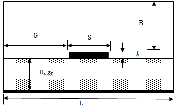
Fig.1 Microstrip Line
G11βnG12βnG21βnG22βnj=1Naj1ρjβnj=1Naj2ρjβn=Vc1βnVc2βn (1a)
(1a)
G11βn=1βnεoεrcothβnH+εo1+cothβntcothβnBcothβnt+cothβnB  (1b)
(1b)
G22βn=1βnεocothβnB+εo1+εrcothβnHcothβntcothβnH+cothβnt  (1c)
(1c)
G12βn=G22βn1sinhβntεrcothβnH+cothβnt  (1d)
(1d)
G21βn=G11βn1sinhβntcothβnt+cothβnB  (1e)
(1e)
The following charge distribution is assumed on strip conductor [12].
ρjx=cosj-1πx-GS1-2x-G-SS2 , G≤x≤G+S (2)
(2)
The capacitance of microstrip line is calculated from following relation [12-14]-
1C=L2εoQ2n=1∞ρj2βnGβn (3)
(3)
Zo=1cCdCair , εreff=CdCair
 (4)
(4)
Gβn=G11βnG12βnG21βnG22βn
where Gβn is Fourier transform of modified Green’s function and ρj
  is Fourier transform of charge distribution present on microstrip line conductor. Q is total charge present on microstrip line. Velocity of light is ‘c’. Cd and Cair are capacitance on dielectric substrate and air substrate respectively.
III. DISPERSION, DIELECTRIC LOSS AND CONDUCTOR LOSS COMPUTATION
Different dispersion models are available to compute frequency dependent effective relative permittivity and impedance. The Kirschning and Jansen Dispersion model is used to compute frequency dependent effective relative permittivity of microstrip line [11].
εrefff=εr-εr-εreff01+Af (5a)
(5a)
Af=A1A20.1844+A3A4fH1.5763 (5b)
(5b)
A1=0.274880.6315+0.5251+0.0157fH2SH-0.065683exp-8.7513SH (5c)
(5c)
A2=0.336221-exp-0.03442εr (5d)
(5d)
A3=0.0363exp-4.6SH1.0-exp-fH38.74.97 (5e)
(5e)
A4=1+2.7511.0-exp-εr15.9168 (5f)
(5f)
fH=f.H=normalized frequency in GHz.mm , 1≤SH≤100 and 1≤εr≤100
  (5g)
(5g)
Zefff=Zoεrefff (5h)
(5h)
The distributed transmission line parameters are used to compute dielectric loss and conductor loss. The dielectric loss is computed from distributed conductance (G) and the relation is given by [1].
αd=GZo2 (6a)
(6a)
G=σ?SH1.08+π1log8HS+1-S8H1.0811.08 (6b)
(6b)
σ?=2πfεoεrtanδ (6c)
(6c)
Conductor loss is due to finite conductivity of the microstrip line. The conductor loss is computed from the total distributed resistance (Rt) and the relation is given by [1]. The total ohmic resistance (Rt) is equal to sum of dc resistance (Rdc) and ac resistance (Rac).
αc=Rt2Zo (7a)
(7a)
αc=Rdc+Rac2Zo (7b)
(7b)
The dc and ac resistance of microstrip line is related to conductivity (σ) and cross section dimension of microstrip line by the following relation [1].
Rdc=1σSt, Rac=1σδS+t (7c)
(7c)
skin depth δ=1πfσμoμr (7d)
(7d)
IV. NUMERICAL RESULT AND DISCUSSION
In this analysis, the microstrip line is present on the cyclic-olefin copolymer dielectric substrates. The relative permittivity, loss tangent and thickness of dielectric substrate are εr = 2.35, tanδ = 5.0×10⁻⁴ and H = 10μm, 20μm respectively. The impedance, effective relative permittivity, dielectric loss and conductor loss are calculated for different width of microstrip line, S=10μm, 20μm, 30μm, 40μm and 50μm on different substrate thickness, H = 10μm, 20μm in the frequency range from 100GHz to 300GHz. The conductivity of microstrip line conductor is 5.618×10⁷ S/m. Fig. 2(a) and Fig. 2(b) shows the variation of impedance and effective relative permittivity with frequency on H=10μm dielectric substrate. The variation of impedance and effective relative permittivity with frequency is very small. This shows the dispersion for microstrip line on cyclic-olefin copolymer substrate is negligible for this wide range of frequency band. Microstrip line and components can be designed in this large frequency bandwidth.
Fig. 2(c) and Fig. 2(d) shows the variation of dielectric loss and conductor loss with frequency. The dielectric loss is very small and increases with frequency. The dielectric loss is small due to small loss tangent. The conductor loss more than dielectric loss. Therefore, major loss in microstrip line is due to conductor loss. The dielectric loss is more for wider microstrip line, but conductor loss is more for narrow microstrip line. Fig. 3(a) and Fig. 3(b) shows the dispersion characteristics of microstrip line on H=20μm dielectric substrate. The characteristic impedance of microstrip line is 88.1ohm and 117.9ohm for H=10μm and H=20μm respectively for S=10μm at 100Ghz. Microstrip line on H=10μm and H=20μm shows the very small dispersion characteristics. The impedance changes with strip width and dielectric substrate thickness.
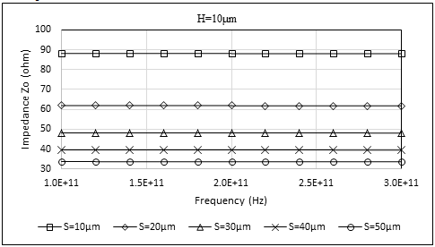
Fig. 2(a) Impedance Zo (ohm), H=10μm, εr=2.35
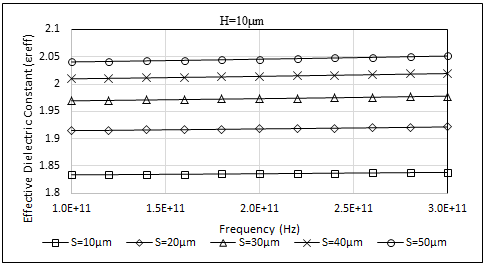
Fig. 2(b) Effective relative permittivity, H=10μm, εr=2.35
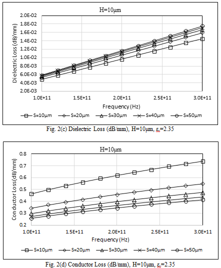
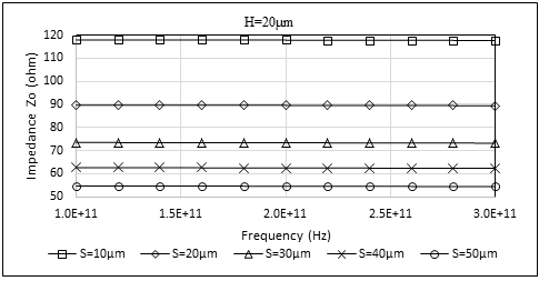
Fig. 3(a) Impedance Zo (ohm), H=20μm, εr=2.35
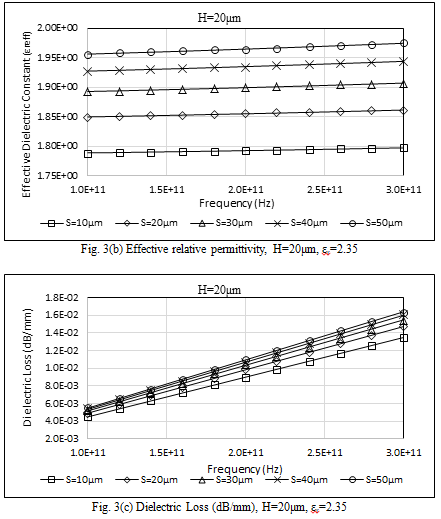
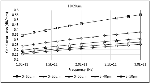
Fig. 3(d) Conductor Loss (dB/mm), H=20μm, εr=2.35
Conclusion
In this paper, the dispersion characteristics of microstrip line, dielectric loss and conductor loss on different thin film dielectric substrate and strip width are analyzed from 100GHz to 300GHz. The microstrip line on thin film dielectric substrate shows the extremely small dispersion. The dielectric losses are also very small compared to conductor loss. Microstrip lines on thin film dielectric substrate are used for wide range of frequency due to low dispersion characteristics and losses.
References
[1] Yong Zhang, Jinyu Zhang, Ruifeng Yue and Yan Wang, Loss Analysis of Thin Film Microstrip Line With Low Loss at D Band, Journal of LightWave Technology, Vol. 39, No. 8, April 15, 2021, pp. 2421-2430. [2] E. Peytavit, C. Donche, S. Lepilliet, G. Ducournau and J. F. Lampin, Thin Film Transmission Lines using Cyclic Olefin Copolymer for Millimeter-Wave and Terahertz Integrated Circuits, Electronics Letters, Vol. 47, No. 7, 31 March 2011. [3] Andrew D. Fund, William B. Kuhn, J. Ambrose Wolf, Ryan J. Eatinger, Kaoru U. Porter, Michael D. Glover and H. Alan Mantooth, Metal Layer Losses in Thin-Film Microstrip on LTCC, IEEE Transactions on Components, Packaging and Manufacturing Technology, Vol. 4, No. 12, December 2014, pp. 1956-1962. [4] George E. Ponchak and Alan N. Downey, Characterization of Thin Film Microstrip Lines on Polymide, IEEE Transactions on Components, Packaging and Manufacturing Technology, Part-B, Vol. 21, No. 2, May 1998, pp. 171-176. [5] Anne-Laure Franc, Emmanuel Pistono and Philippe Ferrari, Characterization of Thin Dielectric Films up to Mm-Wave Frequencies Using Patterned Shielded Coplanar Waveguide, IEEE Microwave and Wireless Components Letters, Vol. 22, No. 2, February 2012, pp. 100-102. [6] C. C. Chen, B. F. Hung, Albert Chin and S. P. McAlister, High-Performance Bulk and Thin-Film Microstrip Transmission Lines on VLSI-Standard Si Substrates, Microwave and Optical Technology Letters, Vol. 43, No. 2, October 20 2024, pp. 148-151. [7] Jang-Hyeon Jeong, Ki-Jun Son and Young Yun, Basic Study on RF Characteristics of Thin-Film Transmission Lines Employing ML/CPW Composite Structure on Silicon Substrate and Its Application to a Highly Miniaturized Impedance Transformer, Transactions on Electrical and Electronic Materials, Vol. 16, No. 1, February 25 2015, pp. 10-15. [8] Hung-Wei Wu, Yan-Kuin Su, Ru-Yuan Yang, Min-Hang Weng and Yu-Der Lin, Fabrication of Low-Loss Thin Film Microstrip Line on Low-Resistivity Silicon for RF Applications, Microelectronics Journal, Vol. 38, 2007, pp. 304-309. [9] Liang Wang, Guangrui Xia and Hongyu Yu, A Method to Determine Dielectric Model Parameters for Broadband Permittivity Characterization of Thin Film Substrates, IEEE Transactions on Electromagnetic Compatibility, Vol. 63, No. 1, February 2021, pp. 229-236. [10] Wen-Yan Yin, X. T. Dong, Junfa Mao and Le-Wei Li, Average Power Handling Capability of Finite-Ground Thin-Film Microstrip Lines Over Ulta-Wide Frequency Ranges, IEEE Microwave and Wireless Components Letters, Vol. 15, No. 10, October 2005, pp. 715-717. [11] R. K. Hoffmann, Handbook of Microwave Integrated Circuits, Artech House, 1987. [12] Cam Nguyen, Analysis Methods for RF, Microwaves and Millimeter-wave Planar Transmission Lines, John Wiley & Sons, Inc. 2000. [13] A. K. Verma, Paramjeet Singh and Ritu Bansal, Computation of Static and Frequency-Dependent Line Parameters of Multilayer CPW Using Static SDA and Single Layer Reduction Method, International Journal of RF and Microwave Computer-Aided Engineering, Vol. 24, No. 1, January 2014, pp. 18-29. [14] Paramjeet Singh, A. K. Verma and Ritu Bansal, Analysis of Multilayer Coplanar Waveguide with Finite Conductor Thickness, International Journal of Microwave and Optical Technology, Vol. 7, No. 6, November 2012, pp. 380-387.
Copyright
Copyright © 2024 Dr. Paramjeet Singh, Dr. Y. K. Awasthi. This is an open access article distributed under the Creative Commons Attribution License, which permits unrestricted use, distribution, and reproduction in any medium, provided the original work is properly cited.

Download Paper
Paper Id : IJRASET65384
Publish Date : 2024-11-19
ISSN : 2321-9653
Publisher Name : IJRASET
DOI Link : Click Here
 Submit Paper Online