Ijraset Journal For Research in Applied Science and Engineering Technology
- Home / Ijraset
- On This Page
- Abstract
- Introduction
- Conclusion
- References
- Copyright
Modeling and Designing a Combination Lock State Machine by Using VHDL
Authors: Abobkr. H. R. Mohamed, Saleman. A. A. Abobker, Masbah Alsnosi Masbah Eame
DOI Link: https://doi.org/10.22214/ijraset.2024.65029
Certificate: View Certificate
Abstract
Recently, the electronic devices enter our daily life in many places, to make it more convenient. However, the aim of this paper, it will be illustrated how to model and design a digital machine by means of VHDL (Very High Speed Integrated Circuit) Hardware Description Language very high modleng. However, the machine that intended to be designed is a Combination Lock State Machine, one of which its output is activated after a certain binary sequence is received while the other output is dependent on both current and past history of the inputs (Mealy Machine). The design will be carried out via Altera Max+plus II framework or program; in addition to that, the design will be inspected and verified by a simulation waveform to make sure that all the required specification is achieved.
Introduction
I. INTRODUCTION
In the past, electronic circuits were designed by hand and manually laid out. However; large chips or systems are too difficult to design by hand. To overcome this issue, there were invented category of tools for designing and producing electronic systems ranging from printed circuit boards (PCBs) to circuits, which known as Electronic Design Automation (EDA). The EDA term is used for computer-aided design (CAD) of electronic chips or ICs in the field of electrical engineering. Modren industries have increased the usage of EDA programs as a result of continuous requirement of semiconductor technology. The EDA is considered as an umbrella which covers computer-aided design (CAD), computer-aided manufacturing (CAM), and computer-aided engineering (CAE); however, these software tools were developed to design the ICs and systems then verifying their behaviour. In modern control system design using CAD techniques, the design can be summarised by the following block diagram that shown below [1, 2, 3].
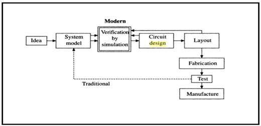
Fig 1: Modern Modelling and Simulation methodology versus traditional approach
On the other hand, the traditional design route starts with idea, and then proceeds to paper circuit design stage. Finally, the prototype design will be tested and verified against the specification that required; however, there are many procedure to test the design (prototyping methods) such as Solderless Breadboard or Plugboard, Springboard, Perfboard and Solder, Generic Printed-Circuit Board—multiple hole-per-pad, “Dead Bug,” or “Ugly-board”….etc. If the result of the simulation is found with a fault, a redesign will be carried out and all the process will be repeated again.
The EDA soft -ware tools enable the design and the evaluation of the complex digital circuit within the built-in computer workstation environment, where the delays are taken into account (hardware is not as a mathematical models), without the requirement of the hardware simulation. By using CAD, can be detect the faults by simulation without going through the costly stage of prototype construction. EDA environment enables us to make any upgrade with the access to the common database. Some of the advantages of EDA include:
- Easier to describe logic and easy to change the design (codes) rather than schematic implementation.
- Save time to design because of reducing the cycle of the design and increasing the abstraction of the design complexity ‘top-down’ design methods.
- In the presence of simulation tools, can get more verification of the design.
- There is a possibility to create alternative designs using synthesis and implementation tools then the designer select the best and the most simplified one for implementation.
There are many programs that can be used in the field of electronic modelling which use the hardware discretion languages such as VHDL and Verilog HDL.In this assignment report, the design of the Machine will be carried out via VHDL approach. Both programs implement the top-down approach that shown in the figure(2); however, at first the design described at register transfer level (RTL) then RTL can be translated into schematics or chip level using synthesis tools. The design procedure is almost as software programming, where the program is written in a high level language before transferring it to machine language. For this reason a hardware description language (HDL) were developed to be implemented in digital industry [1, 3, 5, 9].
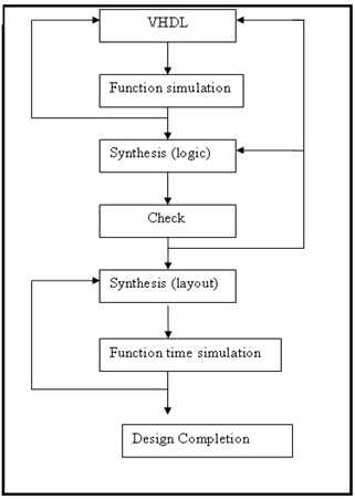
Fig 2: Top-down modeling approach
II. VHDL MODELING
The very high speed integrated circuit (VHSIC) was developed by US government in 1980; however, the VHDL is an enhancement or offshoot virgin to the VHSIC.The aim of these programs is to implement the simplification of digital design process. The designers translate the VHDL as a very hard description language for systems or machines design. The VHDL was standardised with IEEE 1076.1 and the language reference manual (LRM) was published. With the use of the VHDL in designation of ICs, can get many advantages which can be stated as follow:
VHDL programs can be used as a database for different implementation with a little change in the required specifications (reusability).
Has certain standard which reduces the confusion and makes the interface between companies and tools easier.
It has a capability of levels modleing, ranging from transistors to electronic boxes.
It can be commented with the use of two adjacent hyphens to be as a small induction to other users.
There are many terms in VHDL that should be identified before going any further which can be classified as follow:
- Entity: when an entity declared in the program, it will define the interface between the design environment VHDL and a design entity. However; all programs are expressed in terms of entity. The entity specifies all the ports of entity; moreover, the entity-related information.
- Architecture: for every entity there should be architecture which describes the behaviour of entity. A single entity can have multiple architectures. The architecture defines the relationship (behaviour, functionality) between the input and the outputs of the design entity, which can be expressed as a structure or data flow or behaviour.
- Configuration: the configuration statement is used to bind a component instance to an entity-architecture pair. Moreover; it describes which behaviour can be used for each entity. There are two ways for binding components to entity which are soft and hard binding.
- Package: A package is a VHDL unit or toolbox that stores a collection of commonly used data such as types, subtypes, procedures and functions which are pre-defined previously.
- Driver: the driver identified as a source on a signal. In case of a signal is driven by two source, when both of them are active, the signal will have two drivers in that case.
- Bus: the bus is a group of signals which in VHDL is special signals that have their drivers turned off.
- Attrbiute: the attribute defined as the data which attached with VHDL objects or predefined data about VHDL objects. The attributes are used to ease the coding and pass on the information to other design tools an example of that is CLK which written as CLK’ event (means that the Boolean value of CLK is true when the CLK value is changed).
- Generic: In VHDL a generic is the term that used for a parameter which passes the information to entity. The fall and rise delays could be passed into entity via generics.
- Process: the process includes all the operations that performed in simulation; however, the process may break into signals or multiple processes. In the assignment report, there were used two processes, one is used to describe the states of machine and the other one is used to identify the values of inputs and outputs. The process is very important to describe the sequential logic such as Mealy and Moor machines. [1, 10, 11, 6].
III. DESIGN METHODOLOGY AND SIMULATION RESULTS
Before to start the design, it should be put into account all the required specifications; however, the model of the system should cover all the cases in simulation.
IV. SPESIFICATIONS
The machine in general consists of three input ports (X, Reset, CLOCK), and two output ports (UNLK, HINT) as shown in the figure (2, 1). The “UNLK” depends on both the past history and current value of “Xs” while “HINT” values depend on both the state and the current value of the input “X”thus the description can be summarised as a Mealy Machine .The UNLK output should be 1 when “X” is “0” and the sequence that received in the input “X” at the preceding seven clock ticks was “0110111” as indicated in the state and output table (the last row). The HINT output should be “1” with proceeding the following sequence A,B,C,D,E,F,G,H, respectively with the input sequence “0110111” and move the machine to be closer in the “unlocked” state(with UNLK=1).The state and output table can be identified as follow:
In the initial state “A” if the digit that received in the input “X” is “0” the machine will change to the next state “B” while if the input was “1” the machine will stay in the same state. If the machine changed to state “B” and the received input is “1”, the next state will be”C” and if the received input was “0” instead of “1” the machine will stay at the same state. In the state “C”, if the input is “0” ,the next state will be ”B” and it will be changed to the next state”D” with “X=1”.With moving on with required “0110111” sequence, the states will be A, B ,C, D, E, F, G, H. if the input digit is not as the correct sequence ,then the next stat will be “A” or ”B”, but there is an exception in the state “G” where the next state will be ”E”. With reaching the last state “H”, the “UNLK” will be set to “1”.
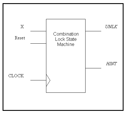
Fig 3: Block diagram of the Lock State Machine
TABLE I
lock state machine state table
|
Meaning |
S |
X |
|
|
0 |
1 |
||
|
Got zip |
A |
B,01 |
A,00 |
|
Got 0 |
B |
B,00 |
C,01 |
|
Got 01 |
C |
B,00 |
D,01 |
|
Got 011 |
D |
E,01 |
A,00 |
|
Got 0110 |
E |
B,00 |
F,01 |
|
Got 01101 |
F |
B,00 |
G,01 |
|
Got 011011 |
G |
E,00 |
H,01 |
|
Got 0110111 |
H |
B,11 |
A,00 |
|
|
|
S*, UNLK HINT |
|
V. DERIVING THE STATE GRAPH
In addition to block diagram and state table the Machine can be represented graphically by a state diagram. In this diagram, a state is represented by a circle, and the transition between states is indicated by directed lines (or arcs) connecting the circles. The letter inside the circle indicates the state while the binary numbers that label the directed line represents “X” input/UNLK, HINT. The state graph that shown above illustrates the entire machine transitions .All the states that indicated in the state table “16” were covered with state graph. With the state graph, can be approach the design and understand all the process of the Machine. In the graph above, there are two different directed lines, the light directed lines represent the correct sequence while the other represents the other 8 states. The reset is connected with state A circle to show that in case of resetting the machine the next state will be A or the Machine Will move on to A state[8, 1].
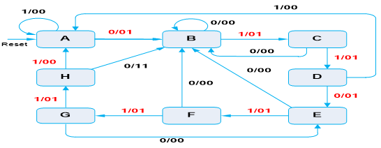
Figu 4: the state graph for the Combination-Lock Machine
VI. PROGRAM SYNTHESIS & VHDL CODS FOR THE DESIGN
First of all, the program should start with the Library code; therefore, all the orders and functions that used in the design were identified in the following library:
Library IEEE;
use ieee.std_logic_1164.all;
The library ieee contains the package (std_logic_1164.all ;).I used the above statements in order that the VHDL compiler knows which library will be used in the design. The next step is that to write entity statement for the program, the entity defines all the ports of the Machine (input and output).in addition to that, it identifies the kind of the port if it is a bit or a vector. The general form of entity or syntax is as follow: [7, 1]
entity NAME_OF_ENTITY is [generic generic_declarations);]
port (signal_names: mode type;
signal_names: mode type;
signal_names: mode type);
end [NAME_OF_ENTITY] ;
The mode is used to identify if the signal is in, out, buffer or inout.The last two types were not used in the modleing; however, the buffer is used to identify that the signal is an output of the entity and its value can be read inside the entity’s architecture, while the inout is used to state declare that the signal can be an input or an output. For the first two steps, can be say that they are almost the same for every program. Should put into account that the name of entity as the name of the file, which the program will be saved in. The next step is that to identify the Architecture body of the program. The design will be implemented for a Mealy Machine thus to achieve a full description to the machine, should give a description of state machine to the design. The description of the machine will be as follow:
- The declaration of the states: Firstly, it was introduced a new type to the program by type declaration, which known as Enumerated Types and it consists of lists of character literals or identifiers. The syntax for an enumerated type is, type type_name is (identifier list or character literal); [7]
- Clocked process: in the clocked process, there will be a description to when and how the states machine should change depending on “X” and the current state values. Moreover, there is a declaration to the behaviour of the machine in the case of being reset. The sensitivity list, here, consists of “clk” and “reset”. The reset action returns the machine to the state “A” in case of the value or digit “1” and “clk” moves on the machine to the next state as shown in the specification table each rising edge [Refer to introduction]. In addition to that, there is a declaration to all states which are listed in the state table (16 states).For the state A, there are 2 possible transitions “A” to “A” or “A” to “B”. for the “B” state is “B” to “B” or “B” to “C”.The identification for the state “C” is “C” or “C” to “B”.the next state is “D”,the transition will be “D” to “E” or “D” to “A”. All the states transition that illustrated in the state graph will be identified by case statement.
- The combinational process: in this part, there will be identification or an assigning for the output values. The output values for “HINT” and “UNLK” is dependent on current state and the input. Thus, the sensitivity list should include as declared in the program (x and state).The state include all the states from “A” to “H” and “X” values are either “0” or “1” with respect to the current state to get the next state.
The sequential statements that were used in the design modleing include the following types:
- If statement: it is similar to any high-level programming language and the condition expression must be have type BOOLEAN. The else portion must be appear one time or not.
- Case statement: it is used in case of a single expression value to choose between a numbers of actions. The case statement is identified, firstly, by keyword case followed by an expression is.
Both expressions can be seen in the programme; however, they are not the only expressions that only the program must execute with. [1, 6, 7, 10, 11].
VII. WAVE-FORM AND SIMULATION RESULTS
To cover all transition of the machine and reset action, there were six wave form of simulation. At each 100 ns the rising edge of the clock moves the states of the machine to the state that must be in according to the state table, which represents the next state. In the first diagram the reset action changed the machine from “B” state to “A”; however; this transition state is not include in the sequential moves. Thus, that proves the reset is working properly as per specification.
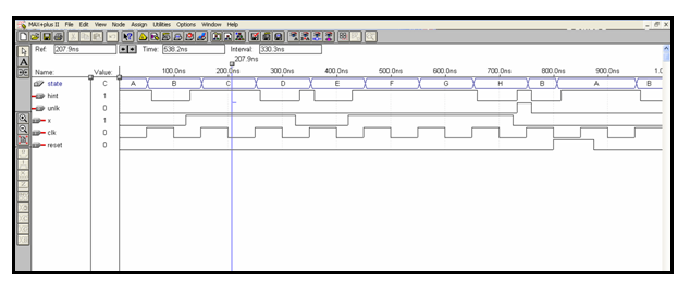
Fig 5: Wave simulation diagram illustrates correct sequence (A to H) and reset action
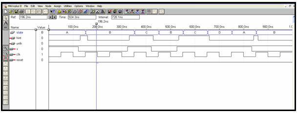
Fig 6: Wave simulation diagram illustrates (B to B), (A to A),(D to A) and(Cto B) states transition
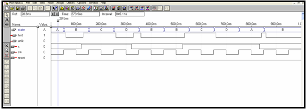
Fig 7: Wave simulation diagram illustrates E to B states transition
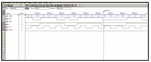
Fig 8: Wave simulation diagram illustrates G to E states transition
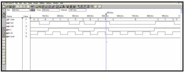
Fig 9: Wave simulation diagram illustrates F to B states transition
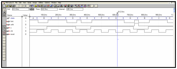
Fig 10: Wave simulation diagram illustrates H to B states transition
All the wave forms that shown above were simulated using Waveform Editor and Simulator. With the results of the wave form simulation, can make sure that the design was completed successfully. The next step is to prototype the design and implements it as a chip [1, 9, 10].
Conclusion
This design was an average of complexity and gave a good example of abstraction for digital circuits design with the use of VHDL modleing. The design was carried out with the highest level of abstraction, which is the behavioural level that describes a system in terms of how it behaves rather than clarifying its components and interconnection between them. With simulating the program and inspecting the results, can judge our design before going to the costly stage which gave an advantage to the program [7, 1].
References
[1] CLEMENTS, Alan. Principles of computer hardware. Oxford University Press, USA, 2006.? [2] Wikipedia Encyclopedia. .Electronic design automation. Retrieved March 27, 2022 from Wikipedia website. [3] http://en.wikipedia.org/wiki/Electronic_design_automation. [4] BIRNBAUM, Mark. Essential electronic design automation (EDA). Prentice Hall Professional, 2004.? [5] CIRSTEA, Marcian, et al. Neural and fuzzy logic control of drives and power systems. Elsevier, 2002.? [6] SCHEFFER, Lou, et al. Electronic design automation for integrated circuits handbook. CRC press, 2006.? [7] Douglas L. Perry, VHDL by Douglas L, April 2, 2022. [8] NO, S. Dr YSR ANU College of Engineering & Technology. Computer, 101: 323.? [9] School of Electrical & Information Engineering, State Tables and State Diagrams, The University of Sydney, 06-Apr-2022. [10] MEANEY, Paul M., et al. Motion based microwave tomographic measurement device for three?dimensional coverage in a magnetic resonance system. Medical physics, 2022, 49.12: 7638-7647.? [11] CHANG, Kou-Chuan. Digital design and modeling with VHDL and synthesis. Los Alamitos: IEEE Computer Society Press, 1997.? [12] MCARDLE, Christopher. The adoption of Application Specific Integrated Circuit (ASIC) technology by the UK manufacturing base. Open University (United Kingdom), 1997.?
Copyright
Copyright © 2024 Abobkr. H. R. Mohamed, Saleman. A. A. Abobker, Masbah Alsnosi Masbah Eame. This is an open access article distributed under the Creative Commons Attribution License, which permits unrestricted use, distribution, and reproduction in any medium, provided the original work is properly cited.

Download Paper
Paper Id : IJRASET65029
Publish Date : 2024-11-06
ISSN : 2321-9653
Publisher Name : IJRASET
DOI Link : Click Here
 Submit Paper Online

