Ijraset Journal For Research in Applied Science and Engineering Technology
- Home / Ijraset
- On This Page
- Abstract
- Introduction
- Conclusion
- References
- Copyright
Non-Isolated High Gain Quadratic Boost Converter
Authors: Shefni ., Rasnas P, Aneesrahman T
DOI Link: https://doi.org/10.22214/ijraset.2025.66261
Certificate: View Certificate
Abstract
A new non-isolated high gain quadratic boost converter is introduced in this paper. The concept of inductors asymmetric input voltage is adopted for developing this high gain converter. The proposed converter benefits from continuous input, positive output, common ground and high-power density features which makes it suitable for renewable energy applications, electric vehicles, dc microgrid applications etc. This converter has got many advantages when compared to the existing topologies in terms of component count, voltage gain, effectiveness index etc. This topology possesses a higher effectiveness index and lower switching device power rating. To validate the performance of the proposed converter, experiments are conducted on 6W laboratory prototype, and corresponding results are presented in this work.
Introduction
I. INTRODUCTION
For several years, switch-mode power converters are being used extensively in modern electronics technology across multiple sectors, including industrial, commercial, utility, and consumer markets.
For low power DC-DC applications, the conversion of power is accomplished using three major types of power converters namely, buck, boost and buck-boost converters. However, certain specialized applications will require advanced combinations or enhanced variations of the conventional topologies. Several DC-DC converters are proposed in the past, but there is no one solution which is suitable for all the applications. In general, conversion techniques have found a wide variety of applications in industry, research and development, and in our daily life.
DC-DC converters is an important aspect in the field of power electronics and energy drives as they are widely used in several industrial applications.
High voltage gain converters are used for multiple applications, which includes radar systems, DC distribution systems, and also renewable energy applications. Nowadays, the whole world is dependent on renewable energy sources for electric power generation due to climatic changes, pollution and mainly the depletion of fossil fuels. Therefore, high gain DC-DC converters are essential or crucial in case of renewable energy applications as it facilitates boosting of the voltage that makes it suitable for integration with the distribution system.
Usually, DC distribution offers a number of advantages including a reduced number of conversion units, price, and improved power quality, which makes it a perfect choice for a good range of applications. It is important to ensure that the design goals of power electronic converters, in general, vary from application to application. However, the most common criteria include maximizing performance and improving power density by reducing the overall cost. Also, the operating conditions need to be taken care of, which includes environmental considerations and operation at a suitable frequency where core losses and switching losses are minimal. Ripple reduction should also be taken care of for both voltage and current, along with heat dissipation and electromagnetic interference so that power density requirements can be fulfilled.
The DC-DC converter topologies employed for renewable energy applications need to draw continuous and smooth input current so that ripple reduction can be achieved. It should also be able to integrate with different types of power sources. Non-isolated interleaved high voltage gain topologies are typically used for interfacing renewables and microgrids.
To achieve high gain DC voltages, boost converters are used. Conventional boost converters use large switching duty cycles to obtain high output voltage. Due to this conduction losses and current stress is increased. Also, the efficiency is drastically reduced with parasitic resistors. The method of cascading proves to be unreliable due to complexity of design. Another method to obtain high output voltage is the inclusion of transformer or coupled inductor. The main disadvantage of this is production of voltage spike, and magnetic interference due to leakage inductance. To overcome these drawbacks, we are introducing a new transformer less or non- isolated high gain quadratic boost converter. This topology introduces the concept of asymmetric input voltage to derive a high voltage gain converter.
II. SYSTEM CONFIGURATION
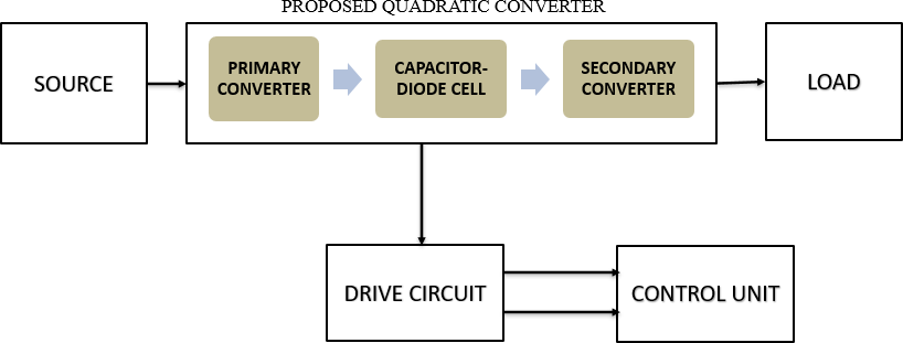
Fig .1. Block Diagram of the system
The block diagram of the proposed high gain non-isolated quadratic boost converter is shown in above figure. The various blocks include; source, the proposed quadratic converter, load, a drive circuit and a control circuit. The input given to the converter is a DC source. The proposed converter consists of two converters in cascaded form; namely, the primary converter and the secondary converter. In between these converters a capacitor-diode cell is incorporated. It consists of a drive circuit which is used to drive the switches and also to isolate the power circuit from the control circuit. The proposed converter consists of two active switches which are operated simultaneously. The control circuit is used to provide the PWM pulses to the synchronously operated active switches.
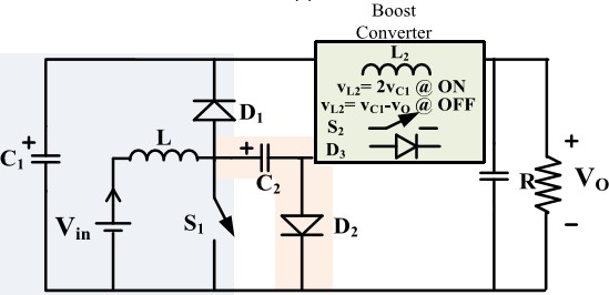
Fig. 2. Schematic diagram of the proposed converter system
The schematic diagram of the proposed converter is shown in figure 2. The proposed converter is derived utilizing diverse input voltage in the ON and OFF states of the secondary converter by integrating the diode-capacitor cell to the conventional quadratic converter.
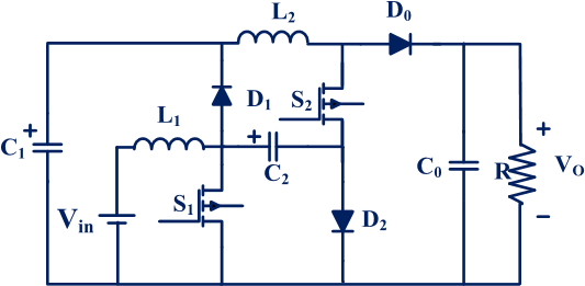
Fig .3 Proposed high gain quadratic boost converter
The assumptions for circuit operation are, all the components used in the circuit are ideal, the capacitors are large enough to maintain output voltage constant, and the converter is operating in continuous conduction mode (CCM). The proposed converter has two modes of operation as described below.
In mode-I (0 < t < DT), the two active switches S1 and S2 will be turned on simultaneously, and the three diodes D1, D2, and D0 will be reversed biased. In this mode, inductor L1 will be energized with the help of the input voltage source Vin and the inductor L2 will get energized with the total voltage supplied by the capacitor C1 and additional capacitor C2. The output capacitor is large enough to support the load current during this mode, and the corresponding power ?ow is shown in figure 4.
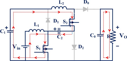
Fig 4. Circuit Structure of Operating Mode 1
Then,
????????1= ???????????? ………………(1)
????????2= ????????1 + ????????2 …………….…(2)
????0= ????????0 ……….………(3)
In mode-II (D < t <T), the two active switches S1 and S2 will be turned off, and the three diodes D1, D2, and D0 will be in conduction as they are forward-biased. The inductors will be demagnetized, and capacitors will get charged in this mode, and the corresponding power ?ow is shown in Figure 5.
Then, the equations are obtained as;
????????1= ???????????? + ????????1
????????2= ???????????? + ????????
????0= ???????????? + ????????1 + ????????2 ……………(4)
Therefore, equation 2 in 4;
????0= ???????????? + ????????1 + ????????1 + ????????2
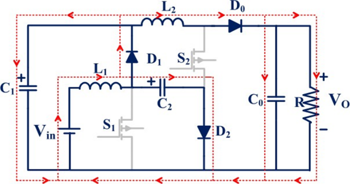
Fig .5. Circuit Structure of Operating Mode 2
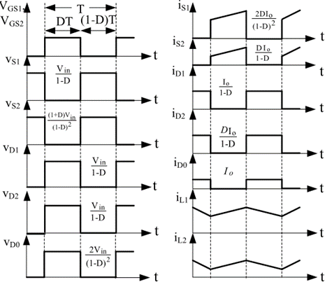
Fig.6. The time-domain waveforms of the converter in CCM
III. PERFORMANCE ANALYSIS OF THE SYSTEM
The proposed non-isolated high gain quadratic boost converter is simulated using MATLAB- Simulink. Designing a converter usually consumes significant time as well as cost. Normally, the performance of the converter is generally determined after testing it at nominal operating points. Therefore, simulation can substantially reduce the development cost.
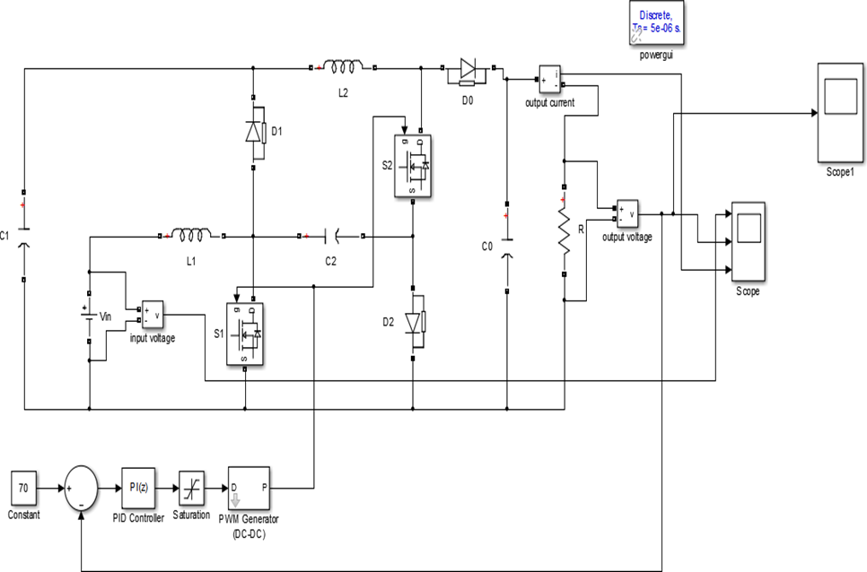
Fig.7. Simulation diagram of the proposed converter
The above figure shows the simulated diagram of the proposed converter. All the components of the converters are selected from the Simulink tools and placed at the right position. Also, a closed loop system is implemented in order to maintain the output voltage constant even if there is any variations in the input voltage or load. Here, a PI controller is used so as to smoothen the output. That is, a PI control mechanism is used to reduce damping and overshoot. After simulating and compiling the converter, the output waveforms obtained are shown in fig 8.
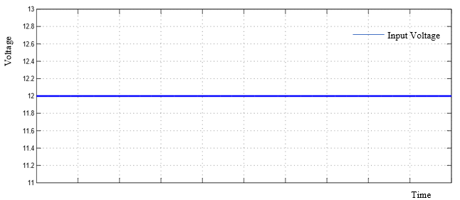
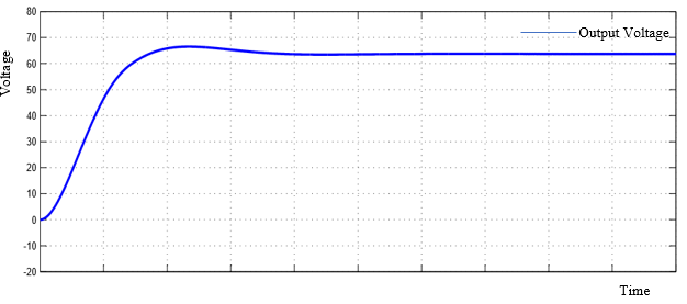
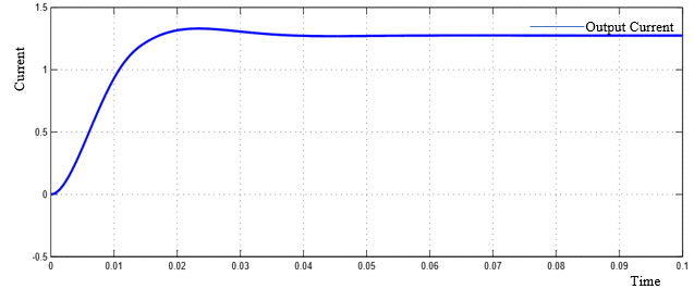
Fig.8. Simulation Waveform
From the above simulated waveforms, we see that for an input voltage of 12V, we obtain 65V output for a load resistance of 100Ω. This shows that the proposed converter is capable to produce an output which is almost five or six times that of the input voltage. Hence, we show that the proposed converter is a high gain converter.
IV. DESIGN OF THE SYSTEM
The below figure represents the schematic of hardware implementation of the control circuit. Here, the microcontroller used is dsPIC30F2010. This microcontroller is used to produce the PWM pulses for two synchronously operated active switches S1 and S2. The TLP250 driver circuit is used to drive the switches and to isolate the control circuit from the power circuit.
dsPIC30f2010 is a 28 pin IC. It requires a supply voltage of 5V which is provided using a regulator IC 7805. Supply is given to Vdd pin of the controller and Vss pin of the controller is grounded. A crystal oscillator pf of frequency 8Mhz is connected across the pins osc1 and osc2 of the controller. Also, two capacitors are connected in parallel with the crystal oscillator.
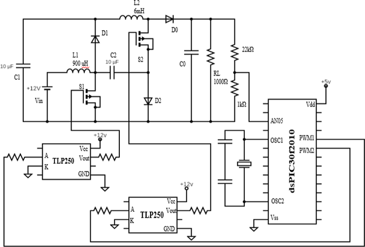
Fig.9. Schematic of the hardware implementation
The circuit consists of two driver circuits as our converter has two switches S1 and S2. TLP250 driver circuits are used in the hardware implantation as shown in the above figure. TLP250 has 8 pins. Two PWM pin connections are taken from dsPIC30f2010 namely, PWM1 and PWM2. Anode pin of one of the TLP250 is connected to PWM1 and the anode of the other driver circuit is connected to PWM2 respectively. Pin 3 which is cathode of the driver circuit is grounded. Also, pin 5 of TLP250 is grounded. Pin 8 i.e., Vcc of TLP250 is given a supply voltage of 12V. Each TLP250 has two output pins which are pin 6 and 7. In one of the drive circuit, pin 7 is connected to the gate terminal of the switch S1 while the pin7 of the other drive circuit is connected to the gate terminal of the switch S2 respectively.
Once, the switches S1 and S2 are provided with the gate pulses, the converter operates and produces output. This output voltage is then scaled down using two resistors as shown in the figure which acts like a voltage divider. Then, this output is fedback to analog pin (AN05) of the controller. It then compares Vref and Vout to produce the corresponding PWM.
A. Design of Passive Components
Switching frequency, fsw = 40kHz
Load resistance, RL = 1000 Ω
Efficiency, η = 90%
Then, the input power is,
Pin = Poutη
 =60.9
=60.9 = 6.67W
P= VI
Input current, Iin = PinVin
 = 6.6712
 = 0.56A
Voltage gain of the converter is,
MCCM = VoutVin
 = 7212
 = 6
= 6
Duty cycle of S1 & S2 is,
D = 1+2MCCM- (1+8MCCM) 2MCCM
= 1+26-√(1+8(6))2(6) = 0.5
= 0.5
Therefore, D = 0.5
Now,
L1 = Vin DΔiL1 fs
ΔiL1 is 30% of IL1
Then, L1 = 12 ×0.50.168 ×40 ×103
 = 893µH
L1≅900 µH
IL2 ≅
≅ Iout1-D
Iout = PoutVout
  = 672
= 672  = 0.0834A
IL2 = 0.08341-0.5
 = 0.167A
ΔiL1 = 0.4×0.167=0.0668A
L2 = 2 ×120.0668 ×40 ×103 0.51-0.5
 = 8mH
= 8mH
L2 ≅6mH
≅6mH
Now, VC1 = VC2
= VC2 = Vin1-D
 = 121-0.5
 = 24V
= 24V
i.e., VC1
VC1 = VC2
= VC2 = 24V
= 24V
Δvc1  is 5% of VC1
Δvc1 = 24 ×0.05 =1.2 V
Then, C1 = Vout Δvc1 R fs
 D1-D
D1-D
C1 = 721.2 ×1000 ×40 ×103 0.51-0.5
C1 = 1.5µF
Similarly, C2 = Vout Δvc2 R fs
 D1-D
D1-D = 1.5µF
C0 = Vout DΔvc0 R fs
VC0 ≅ Vout
Δvc0  = 0.01 ×72=0.72V
C0 = 72 ×0.50.72 ×1000 ×40 × 103
 = 1.25µF
Therefore, the values of all the passive elements are found. The corresponding experimental specifications are shown in the table below.
Table .1. Experimental Specifications
|
Parameter |
specifications |
|
Input voltage |
12V |
|
Inductors |
L1= 900 µH and L2 = 6mH |
|
Capacitors |
C1 = C2 = 10µF, C0 = 1000 µF |
|
Load resistance |
1000Ω |
|
Output power |
6W |
|
MOSFET |
P55 and IRF530 |
|
Diode |
HF04 |
|
Microcontroller |
dsPIC30f2010 |
|
Driver circuit |
TLP250 |
|
Switching frequency |
40kHz |
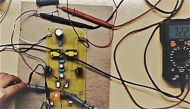
Fig.10. Prototype Testing
To validate the performance of the proposed high gain quadratic boost converter, experiments are conducted on the 6W laboratory prototype as shown in fig. 10. Also, fig. 11 shows the output voltage waveform and fig.12 shows the gate signals of switches S1 and S2 respectively when connected to 1000Ω resistive load.

Fig.11. Output voltage waveform Fig.12. Gate signals of S1 and S2
Conclusion
Nowadays, the whole world is dependent on renewable power generation and electric vehicles due to varying climatic conditions, pollution and depletion of fossil fuels. A high gain DC-DC converter with continuous input is required to meet the dc bus voltage and loads due to low voltage at renewable power sources. A new high gain non-isolated quadratic boost converter is proposed in this paper. The concept of inductors asymmetric input voltage is adopted for developing this high gain converter. To get the quadratic boost gain, usually two conventional boost converters are connected in cascaded nature, where one converter output is fed to another converter. In this we use an additional capacitor-diode cell in between the two converters to obtain the diverse input voltage in the ON and OFF state of secondary converter. This converter consists of two synchronously operated active switches. It has two modes of operation in continuous conduction mode (i.e., when the switches are in ON and OFF states). The proposed converter has continuous input, provides positive output and common ground. Also, this converter has got many advantages when compared to the existing topologies in terms of component count, voltage gain, effectiveness index etc. This topology possesses a higher effectiveness index and lower switching device power rating. This converter is well suited for renewable energy generation, electric vehicles, avionics and dc microgrid applications. Detailed theoretical models for these converters were derived and practically verified. This methodology can be further investigated to derive new high gain DC- DC converters.
References
[1] M. L. Alghaythi, R. M. O’Connell, N. E. Islam, M. M. S. Khan, and J. M. Guerrero, ‘‘A high step-up interleaved DC–DC converter with voltage multiplier and coupled inductors for renewable energy systems,’’ IEEE Access, vol. 8, pp. 123165–123174, 2020. [2] M. Samiullah, M. S. Bhaskar, M. Meraj, A. Iqbal, I. Ashraf, and H. Komurcugil, ‘‘High gain switched-inductor-double-leg converter with wide duty range for DC microgrid,’’ IEEE Trans. Ind. Electron., vol. 68, no. 10, pp. 9561–9573, Oct. 2021. [3] M. A. Salvador, J. M. de Andrade, T. B. Lazzarin, and R. F. Coelho, ‘‘Nonisolated high-step-up DC–DC converter derived from switched-inductors and switched- capacitors,’’ IEEE Trans. Ind. Electron., vol. 67, no. 10, pp. 8506–8516, Oct. 2020. [4] R. Afzal, Y. Tang, H. Tong, and Y. Guo, ‘‘A high step-up integrated coupled inductor- capacitor DC–DC converter,’’ IEEE Access, vol. 9, pp. 11080–11090, 2021. [5] X. Fan, H. Sun, Z. Yuan, Z. Li, R. Shi, and N. Ghadimi, ‘‘High voltage gain DC/DC converter using coupled inductor and VM techniques,’’ IEEE Access, vol. 8, pp. 131975– 131987, 2020. [6] S. V. K. Naresh and S. Peddapati, ‘‘New family of transformer-less quadratic buck-boost converters with wide conversion ratio,’’ Int. Trans. Electr. Energy Syst., vol. 31, no. 11, pp. 1–21, Nov. 2021. [7] C. G. Zogogianni, E. C. Tatakis, and M. S. Vekic, ‘‘Non-isolated reduced redundant power processing DC/DC converters: A systematic study of topologies with wide voltage ratio for high-power applications,’’ IEEE Trans. Power Electron., vol. 34, no. 9, pp. 8491– 8502, Sep. 2019. [8] R. Panigrahi, S. K. Mishra, and A. Joshi, ‘‘Synthesizing a family of converters for a specified conversion ratio using flux balance principle,’’ IEEE Trans. Ind. Electron., vol. 68, no. 5, pp. 3854–3864, May 2021. [9] S. B. Mahajan, P. Sanjeevikumar, P. Wheeler, F. Blaabjerg, M. Rivera, and R. Kulkarni, ‘‘X-Y converter family: A new breed of buck boost converter for high step-up renewable energy applications,’’ in Proc. IEEE Int. Conf. Autom. (ICA-ACCA), Oct. 2016, pp. 1–8. [10] S. Ding and F. Wang, ‘‘A new negative output buck–boost converter with wide conversion ratio,’’ IEEE Trans. Ind. Electron., vol. 64, no. 12, pp. 9322–9333, Dec. 2017. [11] J. C. Mayo-Maldonado, J. E. Valdez-Resendiz, P. M. Garcia-Vite, J. C. Rosas-Caro, M. D. R. Rivera-Espinosa, and A. Valderrabano-Gonzalez, ‘‘Quadratic buck–boost converter with zero output voltage ripple at a selectable operating point,’’ IEEE Trans. Ind. Appl., vol. 55, no. 3, pp. 2813–2822, May/Jun. 2019. [12] V. C. Mummadi and M. R. Khuntia, ‘‘Design and analysis of two-switch based enhanced gain buck-boost converters,’’ IEEE Trans. Ind. Electron., early access, Apr. 13, 2021, doi: 10.1109/TIE.2021.3071696. [13] J. Li and J. Liu, ‘‘A novel buck–boost converter with low electric stress on components,’’IEEE Trans. Ind. Electron., vol. 66, no. 4, pp. 2703–2713, Apr. 2019. [14] M. Veerachary and N. Kumar, ‘‘Analysis and design of quadratic following boost converter,’’ IEEE Trans. Ind. Appl., vol. 56, no. 6, pp. 6657–6673, Nov. 2020. [15] Y. Wang, Y. Qiu, Q. Bian, Y. Guan, and D. Xu, ‘‘A single switch quadratic boost high step-up DC–DC converter,’’ IEEE Trans. Ind. Electron., vol. 66, no. 6, pp. 4387–4397, Jun. 2019 [16] M. L. Alghaythi, R. M. O’Connell, and N. E. Islam, ‘‘Design of a high step-up DC–DC power converter with voltage multiplier cells and reduced losses on semiconductors for photovoltaic systems,’’ in Proc. IEEE Electric Ship Technol. Symp. (ESTS), Aug. 2019, pp. 214–218. [17] A. Alzahrani, M. Ferdowsi, and P. Shamsi, ‘‘A family of scalable non-isolated interleaved DC-DC boost converters with voltage multiplier cells,’’ IEEE Access, vol. 7, pp. 11707–11721, 2019. [18] M. S. Bhaskar, V. K. Ramachandaramurthy, S. Padmanaban, F. Blaabjerg, D. M. Ionel, M. Mitolo, and D. Almakhles, ‘‘Survey of DC–DC non-isolated topologies for unidirectional power flow in fuel cell vehicles,’’ IEEE Access, vol. 8, pp. 178130–178166, 2020. [19] M. Forouzesh, P. Y. Siwakoti, A. S. Gorji, F. Blaabjerg, and B. Lehman, ‘‘Step-up DC–DC converters: A comprehensive review of voltage-boosting techniques, topologies, and applications,’’ IEEE Trans. Power Electron., vol. 32, no. 12, pp. 9143–9178, Dec. 2017. [20] G. G. Kumar, K. Sundaramoorthy, V. Karthikeyan, and E. Babaei, ‘‘Switched capacitor–inductor network based ultra-gain DC–DC converter using single switch,’’ IEEE Trans. Ind. Electron., vol. 67, no. 12, pp. 10274–10283, Dec. 2020. [21] A. Sarikhani, B. Allahverdinejad, and M. Hamzeh, ‘‘A nonisolated buck– boost DC– DC converter with continuous input current for photovoltaic applications,’’ IEEE J. Emerg. Sel. Topics Power Electron., vol. 9, no. 1, pp. 804–811, Feb. 2021. [22] K. Yari, S. H. Shahalami, and H. Mojallali, ‘‘A novel nonisolated buck– boost converter with continuous input current and semiquadratic voltage gain,’’ IEEE J. Emerg. Sel. Topics Power Electron., vol. 9, no. 5, pp. 6124–6138, Oct. 2021. [23] J. Leyva-Ramos, R. Mota-Varona, M. G. Ortiz-Lopez, L. H. Diaz-Saldierna, and D. Langarica-Cordoba, ‘‘Control strategy of a quadratic boost converter with voltage multiplier cell for highvoltage gain,’’ IEEE J. Emerg. Sel. Topics Power Electron., vol. 5, no. 4, pp. 1761–1770, Dec. 2017. [24] A. Mahmood, M. Zaid, J. Ahmad, M. A. Khan, S. Khan, Z. Sifat, C.-H. Lin, A. Sarwar, M. Tariq, and B. Alamri, ‘‘A non-inverting high gain DC-DC converter with continuous input current,’’ IEEE Access, vol. 9, pp. 54710–54721, 2021. [25] X. Zhu, K. Ye, K. Liu, and B. Zhang, ‘‘Non-isolated high step-up DC–DC converter with passive switched-inductor-capacitor network,’’ IEEE J. Emerg. Sel. Topics Power Electron., early access, Nov. 13, 2021, doi: 10.1109/JESTPE.2021.3125403.
Copyright
Copyright © 2025 Shefni ., Rasnas P, Aneesrahman T. This is an open access article distributed under the Creative Commons Attribution License, which permits unrestricted use, distribution, and reproduction in any medium, provided the original work is properly cited.

Download Paper
Paper Id : IJRASET66261
Publish Date : 2025-01-03
ISSN : 2321-9653
Publisher Name : IJRASET
DOI Link : Click Here
 Submit Paper Online


 = 12V
= 12V = 72V
= 72V = 6W
= 6W =
= 
 0.3 = 0.168A
 D1-D
D1-D