Ijraset Journal For Research in Applied Science and Engineering Technology
- Home / Ijraset
- On This Page
- Abstract
- Introduction
- Conclusion
- References
- Copyright
A PFC based EV Battery Charger using a Bridgeless Isolated SEPIC Converter
Authors: Mr. A. Vinothkumar, M. S. Deepika, V. Kaviya Priya, V. Gowarna Jayasri
DOI Link: https://doi.org/10.22214/ijraset.2023.51177
Certificate: View Certificate
Abstract
Conventional PFC circuits in EV (Electric Vehicle) battery chargers have efficiency limitations. To overcome this issue, there were losses associated with the DBR, hence a bridgeless single-ended primary inductance converter (SEPIC) with improved power quality is presented in this project. The input current drawn by the charger shows a unity power factor operation in a complete switching cycle. Due to the elimination of DBR, conduction losses are significantly controlled. The overall performance of the proposed bridgeless SEPIC converter is analyzed with the help of various operating modes. The EV battery is charged at constant current/ constant voltage control mode, which provides satisfactory results for improved efficiency and inherent PFC, thus improving the overall performance of the charger.
Introduction
I. INTRODUCTION
Due to the expanding trend of eco-friendly design, LED lighting is gaining support in lighting applications. As a result, the power quality of LED lighting has emerged as a critical topic in power electronics. Figure 1.1 is a block schematic of a typical LED lighting system. A high alternating current voltage is passed through an ac/dc PFC stage, which rectifies the alternating current to direct current, and the PFC control delivers high-quality power for the LED lighting system. The input of the dc/dc converter is the output of the ac/dc PFC stage, and the output of the dc/dc converter creates a low-input voltage for the LED lighting module, which normally requires an input voltage ranging from 12V to 50V. As illustrated in Figure 1.1, the PFC stage is required and critical.\

Power factor is expressed as follows:
PF = cos(Tita)
where: (Tita: phase difference between input current and input voltage)
The PFC stage is also critical in avoiding input power loss. Input power loss may be caused by input current harmonics. A PFC aligns the input current and voltage sine waves. When PF is 1.0, the input current is exactly in phase with the input voltage, with little current distortion. Because of the low power loss, the system can be extremely efficient.
The second reason for the present focus on PFC is to meet international standard criteria such as EC-62000-3-2. The single-ended primary-inductance converter (SEPIC) is a DC-to-DC converter topology that generates a positive regulated output voltage from an input voltage that ranges between the output voltage and zero. When the designer uses voltages (e.g., 12 V) from an unregulated input power supply, such as a low-cost wall wart, this form of conversion comes in handy. Unfortunately, the SEPIC topology is difficult to understand and requires two inductors, resulting in a huge power supply footprint. Several inductor manufacturers have recently begun providing off-the-shelf linked inductors in a single package at prices just marginally higher than a similar single inductor. Active power factor correction (PFC) circuits are extensively used in ac-dc converters and switched-mode power supplies to meet the demand for high efficiency and reduced harmonic pollution. In general, these converters comprise a full-bridge diode rectifier on an input current channel, resulting in conduction losses on the full-bridge diode, which are worse at the low line. Bridgeless converters have lately been introduced to reduce or eliminate the full-bridge rectifier and hence their conduction losses. The SEPIC has been intended to improve power factor correction in ac systems in order to attain a high-power factor. A portion of the SEPIC input voltage and current has been utilized, lowering the amount of lower-order harmonics and producing a high-power factor.
For high power factor under conditions of universal input voltage, a new bridgeless PFC SEPIC converter has been developed. via integrating this topology into the DCM SEPIC derived converter, a novel PFC topology has been produced via the valley-fill circuit. The issue with the bus capacitor voltage being dependent on output load was resolved, and excessive voltage stress under light load was avoided. By combining SEPIC compression with a CUK PFC converter, two innovative single phase bridgeless rectifiers with little input current distortion and low conduction losses have been created. The obtained SEPIC converter efficiency has increased due to the smaller inductor size. Due to the constantly rising number of electronic devices, there is a growing need to improve the ac system's power quality. equipment. Power factor correction (PFC) research became a hot topic in power electronics, and substantial efforts have been made on the advancements of the PFC converters in order to decrease harmonic contamination in power lines and increase transmission efficiency. In fact, as more stringent power quality requirements and strict limits on the total harmonic distortion (THD) of input current are imposed, PFC circuits are becoming required on single-phase power supplies. Single-ended primary inductor converter is referred to as a SEPIC.
It is a particular kind of DC-DC converter that is utilized in numerous other applications, including DC power supply, electronic ballasts, telecommunications, and battery chargers for mobile phones. Due to zero voltage switching and synchronous rectifier operation, it features low switching and conduction losses. The single-ended primary inductor converter, often known as SEPIC, is used to boost, buck, or maintain the supply voltage. By altering the duty cycle of power switches like MOSFETs, IGBTs, GTOs, etc., the SEPIC output can be managed. It has an extra benefit over conventional buck-boost converters in that the output is not inverted (the output has the same polarity as the input). In order to relate energy from input to output and enable true shutdown, series capacitors are used.
II. SYSTEM ANALYSIS
A. SEPIC Converter
To improve the efficiency of the conventional boost-type power factor correction (PFC) converters with the diode bridge circuit, the PFC converters of the bridgeless category are often used. Due to no series-connected switches and no short-through risks, the dual-boost half-bridge (DBHB) circuit is used as the PFC converter in this paper. In order to simplify the conventional two-loop control scheme and reduce the number of sensors, the behaviors of the DBHB PFC converter are studied and its equivalent single-switch model is developed. In addition, the proposed method is able to balance capacitor voltages naturally without adding any voltage-balancing control loop. An 800W DBHB PFC prototype is implemented to evaluate the control performance. Both simulation and experimental results are provided to demonstrate the proposed current sensor-less control method.
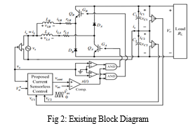
The single-switch model for DBHB PFC converter has been developed. The current sensor-less control method for DBHB PFC converter has been proposed and implemented in this paper. The integrator-type voltage controller is able to regulate the output voltage and balance the capacitor voltages. The proposed control strategy effectively achieves PFC function in steady-state condition and transient condition. Moreover, the capacitor voltages can be naturally balanced by the proposed control method. From the simulation and experimental results of 800W prototype converter, the proposed current sensor-less control method is demonstrated. Dual-boost half-bridge (DBHB) PFC converter with the proposed current sensor-less control For PFC application, the conventional two-loop control with the inner current loop and the outer voltage loop can be used to control all the converters in Fig. 1 where it needs to sense the DC-link voltage, the AC voltage and the inductor current. It is noted that the two-loop control can also be used in the half-bridge converters, but it needs to include third control loop to balance both capacitor voltages.
Therefore, total four sensors (three voltage sensors and one current sensor) are needed to implement the half-bridge PFC converter. In digital PFC control, the current is conventionally feedback by the current sensor and Analog-to-Digital converter (ADC) with high resolution and high bandwidth. To reduce the cost, some control methods had been proposed in. In the current sensing methods using only comparators without real A/D converter were proposed. Furthermore, the control methods proposed in rebuilt the current feedback signal from the sensed voltages. An adaptive inductor model and the adaptive nonlinear current observer were developed to estimate the current, individually. All the above methods can be classified into two-loop current sensor-less control methods.
B. Proposed System
Due to increasing concerns on the power quality, power factor correction (PFC) has become an important issue in light-emitting diode (LED) lighting applications. A boost converter is one of the most well-known PFC topologies, due to its simple circuitry, simple control scheme and small number of passive components. Even though a boost converter is recognized as a typical PFC converter, its output voltage must be higher than its input voltage.
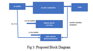
This feature is disadvantageous because the device requires an additional buck-stage for LED lighting systems. As an alternative to the boost converter, a single-ended primary-inductor converter (SEPIC) allows output voltage to be lower or higher than the input voltage. Thus, the SEPIC converter is gaining popularity as a LED driver because it does not require additional power conversion stage. However, designing a controller to meet stability requirements and international standards is quite challenging for SEPIC converters. Additionally, if the digital controller is adopted for its built-in communication features, creating a digitally controlled SEPIC converter would be even more challenging. This thesis focuses on the state-space averaging modeling of the SEPIC PFC converter and the design of controllers based on both analog and digital controls with precise modeling. The proposed SEPIC converter incorporates RC damping circuits to avoid the instability, and thus the entire SEPIC converter becomes a 5th order system. After verification of the circuit model, the controller was designed with analog transfer functions and converted to and the discrete domain for digital controller implementation. Bridgeless SEPIC PFC converter prototype was built accordingly to verify the design. The ZVS & ZCS topology reduces the switching loses with the help of resonant networks. In addition to the current loop controller design for stability, a Fuzzy logic compensator for is introduced and derived for better waveform quality. Simulation results and experiment results are also presented to verify the complete controller with feed-forward compensation. The Microchip digital signal peripheral Interface controller DSPIC30F2010 controller was adopted for digital controller implementation.
C. Circuit Diagram
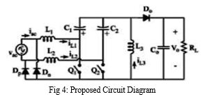
The input AC voltage is given to the bridgeless SEPIC harmonics. This DC voltage is fed to the Single-phase inverter To reduce the switching losses resonant converters are proposed. The figure shows the proposed system circuit diagram. The features of resonant converters are zero current switching (ZCS), zero voltage switching (ZVS), and efficiency is high, size will be small and there are no EMI problems. Resonant converters are successfully applied to AC power supplies for improving the power factor and heating, DC power supplies for domestic and industrial applications. There are two types of basic resonant converters series and parallel RC. The series RC has better part load efficiency and lack of DC blocking voltage of the transformer due to the series connected capacitor in RC. But, its load regulation is poor and output voltage regulation is not possible in the no-load condition. But, the PRC offers good no-load regulation and load efficiency is poor and lack of DC blocking of the transformer the AC L-C-L resonant network formed with the components ????1, ????1 ???????????? ????2, along with the planar transformer connected at output stage and it provide isolation. The values of inductances and capacitance are chosen for the AC L-C-L resonant network are resonance at the output frequency of MLI. ???????? = ????1 + ????2 from above equation voltage across????1 will be ????2 and the voltage across ????2 will be????1.
The output current of AC L-C-L resonant network, ????2, can be controlled by controlling the multilevel-inverter output voltage ????1.For, electroplating process require the power supply low voltage DC and high current DC, but multilevel inverter output voltage is very high. So by using L-C-L resonant converter the output voltage can be reduces. Furthermore, the multilevel inverter output voltage ????1 is more compare to L-C-L network output voltage ????2. But the, merit of L-C-L resonant converter is to maintain the constant current source, that means current through ????1 is equal to the current through ????2i.e ????1 = ????2. Further, the output of AC L-C-L resonant converter connected to primary winding of planar transformers. In order to increase the current levels, the planar transformer connected in the shown in fig above. That means there are eight transformers connected in primary side series and secondary side parallel with center tapped for isolation purpose. Primary windings are connecting in series the high voltage can be distributed each of primary winding with an equal voltage distribution assured by connecting the secondary side windings in parallel. Similarly, the parallel connection the high current to be distributed each of secondary winding with an equal current assured by connecting the primary in series.

V. FUTURE SCOPE
- The fuzzy logic controller output voltage still having oscillations. The Neuro fuzzy logic algorithm provides efficient results.
- Instead of normal three level inverter, multi level inverter can reduce the THD in the output voltage.
Conclusion
The proposed project inherits all the drawbacks of the existing system. The bridgeless topology reduces the source current harmonics. The SEPIC converter maintains constant voltage to the load. The PI PWM topology achieves constant DC output voltage with respect to load variation. The single-phase inverter will converter the DC to AC voltage, the isolation transformer will reduce the primary side non isolated current. The synchronous rectifier can vary the output voltage of the DC side. The BLSEPIC converter is used to achieve the good power factor correction and efficiency of the system.
References
[1] Y. Suresh, A.K Panda, “Research on Cascaded Multilevel Inverter by Employing Three- Phase Transformers,” IET power electronics, vol. 5, pp. 561-570, 2012. [2] Zhong Du, Tolbert, Chiasson, “A cascade multilevel inverter using a single DC source”, Applied Power Electronics Conference and Exposition. (APEC), 2006. [3] P. Yunqing, J. Guibin, L. Haitao, and W. Zhaoan, \"Development of high current power supplies for electroplating,\" Proc. Power Elec. Spec. Conf. (PESC), 2002, vol.1, pp. 21-23. [4] Z. Weimin, D. Minghai, P. Yunqing, and W. Zhaoan, \"Design and optimization of high current power supply for electrochemistry,\" Proc. Power Elec. Conf. (IPEC), 2010, pp. 86-91 [5] S. Lejia, H. Jun, P. Yunqing, and W. Zhaoan, \"Design and optimization of high current intelligent waveform power supply for electroplating”, Proc. Power Elec. and Motion ControlConf. (IPEMC), 2012, pp. 1516-1521 [6] L. Jih-Sheng and P. Fang Zheng, \"Multilevel converters-a new breed of power converters,\" IEEE Trans. Ind. App., 1996, vol. 32, pp. 509-517 [7] L. M. Tolbert, F. Z. Peng, and T. G. Habetler, “Multilevel converters for large electric drives”, IEEE Trans. Ind. Appl., 1999, vol. 35, pp. 36–44 [8] J. Rodriguez, J.-S. Lai, and F. Z. Peng, “Multilevel inverters: A survey of topologies, controls, and applications”, IEEE Trans. Ind. Electron., 2002, vol. 49, pp. 724–738. [9] B. W. Carsten, \"The low leakage inductance of planar transformers; fact or myth?,\" Proc. Applied Power Elec. Conf. and Expo. (APEC), 2001, vol.2, no., pp.1184-1188. [10] U. K. Madawala and D. J. Thrimawithana, \"Modular-based inductive power transfer system for high-power applications,\" IET Power Electronics., 2012, vol. 5, pp. 1119-1126 [11] U. K. Madawala and D. J. Thrimawithana, \"New technique for inductive power transfer using a single controller,\" IET Power Electronics., 2012, vol. 5, pp. 248-25. [12] M. Borage, S. Tiwari, and S. Kotaiah, \"Analysis and design of an LCL-T resonant converteras a constant current power supply,\" IEEE Trans. Ind. Elec., 2005, vol. 52, pp. 1547-1554 [13] M. Borage, K. V. Nagesh, M. S. Bhatia, and S. Tiwari, \"Design of LCLT Resonant Converter Including the Effect of Transformer Winding Capacitance,\" IEEE Trans. Ind. Elec.,2009, vol. 56, pp. 1420-1427. [14] A. Bhat, “Analysis and design of LCL-type series resonant converter,” IEEE Trans. Ind.Elec., 1994, vol. 41, pp. 118-124. [15] S. Raabe, J. T. Boys, and G. A. Covic, \"A high power coaxial inductive power transfer pickup,\" Proc. Power Elec. Spec. Conf, (PESC), 2008, pp. 4320-4325. [16] U. K. Madawala, M. Neath, D. J. Thrimawithana, \"A Power–Frequency Controller for Bidirectional Inductive Power Transfer Systems,\" IEEE Trans. Ind. Elec., Jan. 2013, vol.60, no.1, pp.310-317. [17] Muhammad H. Rashid, “Power Electronics Circuits, Devices and Applications, 3rd ed., PEARSON publication, 2009. [18] V. Naga Bhaskar Reddy, V. Narasimhulu, “Control of Cascaded Multilevel Inverter by using carrier based PWM technique and implemented to Induction Motor drive,” International Journal on Automatic Control and System Engineering (ICGST-ACSE Journal), vol. 10, Issue 1,Dec 2010. [19] Jagdish Kumar, Biswarup Das, and Pramod, “Selective Harmonic Elimination technique for a Multilevel inverter,” in Proc. of 15th National Power Systems Conference (NPSC), IIT Bombay, pp. 608-613, 16-18Dec 2008.
Copyright
Copyright © 2023 Mr. A. Vinothkumar, M. S. Deepika, V. Kaviya Priya, V. Gowarna Jayasri. This is an open access article distributed under the Creative Commons Attribution License, which permits unrestricted use, distribution, and reproduction in any medium, provided the original work is properly cited.

Download Paper
Paper Id : IJRASET51177
Publish Date : 2023-04-28
ISSN : 2321-9653
Publisher Name : IJRASET
DOI Link : Click Here
 Submit Paper Online

