Ijraset Journal For Research in Applied Science and Engineering Technology
- Home / Ijraset
- On This Page
- Abstract
- Introduction
- Conclusion
- References
- Copyright
Preparation and Characterization Studies of CU2SnS3 Thin Film using Ultrasonic Spray Pyrolysis Technique for Solar Cell Application
Authors: S Pranisha
DOI Link: https://doi.org/10.22214/ijraset.2024.64047
Certificate: View Certificate
Abstract
Low-cost ternary chalcogenide is produced using technologies like ultrasonic pyrolysis spray method. A thin film of Cu2SnS3 which is doused with the substrate of glass temperature by altering the temperature from 330 C to 550 C. As the temperature increases, the amorphous phase of the thin layer of Cu2SnS3 crystal structure is discovered to shift to tetragonal phase. Using this above technique Cu2SnS3 chalcogenide thin film were deposited at temperature of substrate, varying from 300 C to 550 C in increment of 50 C, utilizing affordable, computerized pyrolysis using ultrasonic spray processes. When films are generated at 500 C for the substrate the The tetragonal phase of Cu2SnS3 is produced in highly crystalline films. Higher temperature of substrate results in the develop the binary phase SnS2.650.4 nm is discovered to be the typical film thickness. So, by using pyrolysis technique the attributes of the thin-film Cu2SnS3 is studied in solar cell.
Introduction
I. INTRODUCTION
As non-renewable energy resources become scarce, Solar energy has become recognized as one of the major Renewable energy sources in recent times. Thin-film Solar cells (TLCs) are being developed by numerous Researchers employing solar absorber materials like CdTe, CuInSe2, and CuInGaSe2 (CIGS). A record-Breaking 22.9% The achievement of conversion efficiency using CIGS solar cells manufactured with a two-step Process to date [1]. Kesterites, like Cu2ZnSnSe4(CZTSe), Cu2ZnSnS4 (CZTS), an the vacuum approach for producing thin film of copper zinc tin sulfide for solar cells yielded a efficiency is recorded which is of 10.0 percentage [1]. Synthesising copper zinc tin sulfide thin flim with controlled elements composition to achieve a single kesterite copper zinc tin sulfide phase which is challenging due to the development of binary and ternary phases, including Cu2S, SnS2, Sn2S3, Cu2SnS3, Cu3SnS4, and Cu4SnS4 [2] Cu2ZnSn (SSe)4(CZTSSe), are not as commonly used in solar cell. Applications due to their toxicity, rare earth element content, and high cost. Cu2ZnSnS4 (CZTS) is a possible absorber layer material that can replace existing CIGS and CdTe.CZTS absorber material, a form of kesterite, with a high coefficient of absorption (>104 cm−1), p-type conductivity, and a straight band gap energy between 1.4 to 1.6 eV. These elements are common on earth. As address this issue, ternary substances with comparable crystal structures and opto-electrical properties as CZTS are used. Cu2SnS3 (CTS), a I-IV-VI trivalent chalcogenide molecule semiconductor, is p-type. Solar cells’ photovoltaic properties are affected by flaws, secondary phases, and non-stoichiometric absorber compounds. The single-phase The absorber layer's crystal structure and be devoid of defects. By adjusting the metallic precursors composition, phase control over the layer of absorption can be achieved. Apart from the aforementioned factors, the absorber layer's thickness also significantly influences the the effectiveness of conversion. Owing to its the CTS's phase transition temperature is 780 °C. At higher temperatures, the phase is isomorphic (cubic), but at lower temperatures, the phase is polymorphic (tetragonal, monoclinic, triclinic).In [3]. Adjusting the interval between bands within a 0.9 eV range is a unique capability of CTS.
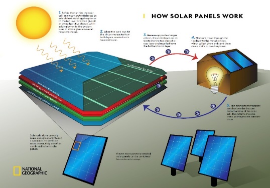
Figure 1: Solar panel
Light photons can readily enter the p-n junction through the extremely thin p-type layer when light reaches the junction. Photons provide enough vitality for the junction to build several electron-hole pairs. The junction's thermal equilibrium is broken by the Incident light. The n-type side of the junction can rapidly receive the free electrons from the depletion region. This particular research uses the ultrasonic spray top. Narrow distribution size, shorter deposition time, uniform film surface, and gas flow rate independent of aerosol flow rate are some of the benefits of ultrasonic pyrolysis spray technique over traditional spray pyrolysis. Cu-SnO2 has been Effectively synthesized by Alam et al. The produced nanoparticles were applied to H2S sensor detection. By doping Cu2SnS3 films with potassium, Ruan et al. increased their conversion efficiency by ultrasonically sprayed films. The Cu2SnS3 films' phase composition, produced by ultrasonic spray pyrolysis was investigated by Ignacio et al. The automated setup is effective for growing AginS2 and Cu2(Zn,Sn)S4 thin films. This article covers the properties and characteristics of films produced on substrate of glass by altering the temperature of substrate between 300 and 550 °C. Lastly, the improved CTS thin film’s photocatalytic effect is investigated.
II. RELATED WORK
In [1], substrate temperatures were adjusted from 300 °C to 550 °C in order to Cut inexpensive thin films of the ternary chalcogenide Cu2SnS3 (CTS) using ultrasonic spray pyrolysis (USP) on glass substrates. A rise in substrate temperature causes the CTS thin film crystal structure to transition from an amorphous phase to a tetragonal phase. The properties of the Several characterization techniques are applied to evaluate the thin sheets of Cu2SnS3 are deposited. With an increase in substrate temperature, a Experimental results using X-ray powder diffraction (XRD) indicate the formation of a Cu2SnS3 tetragonal phase with orientation along the (112) plane. Binary had formed on the substrate at 550 °C, according to Raman analysis. The stoichiometry of the tin and copper film sulfide was reached at 500 °C when temperature of subtrate was raised. With a band gap of approximately 105 cm-1, the coefficient of absorbance of CTS films.
In [2], the author describes the manufacture of a Heterojunction Cu2SnS3/ZnS photovoltaic cell utilizing an Indigenously developed cost-effective pyrolysis with ultrasonic spray process. The substrate temperatures used in order to create the films ranged from 350 to 500 C. Temperature significantly increased ZnS films' three optical qualities that make them perfect for solar cell window layers. The cell’s p-type Cu2SnS3 (CTS) absorber layer is produced at optimal substrate temperature (500C) with optimized Cu and Sn composition. Finally, a solar cell is Built using these optimized p and n layers, with a structure mA/cm2, fill factor 39%, and solar efficiency = 0.5%. A lengthy explanation on overcoming the complexities.
This work [3] is an example of an affordable technique for ultrasonic spray pyrolysis (USP) is utilized to create Cu2SnS3 (CTS) thin films without toxicity by altering the amount of copper chloride, a copper precursor. The study investigates how Cu concentration affects the structural, electrical, and optical features of thin films CTS. The plane-oriented XRD and TEM examinations of CTS films reveal their tetragonal structure. Analysis of Raman of films with increased Cu content validates the CTS thin film's tetragonal structure and the Cu2S secondary phase. A stoichiometric film is discovered with a concentration of 0.025M Cu. Studies using PL and XPS are also carried out. CTS films have an absorbance coefficient of about 105 cm.
In[4] employed a low-cost spray pyrolysis technique to deposit Cu2ZnSnS4 (CZTS) thin films on soda-lime glass (SLG) and Mo-coated SLG substrates. Sulfurization was conducted at 540°C with H2S flowing. The precursor was an aqueous solution containing thiourea, ZnCl2, CuCl, and SnC14. Three district substrate temperatures-280°C, 360°C, and 440°C were utilized in order to spray deposition. The Ideal film characteristics were achieved by optimizing The deposition circumstances. The as-deposited and sulphurised CZTS Films were investigated using a variety of techniques such as AFM, SEM, EDX, XPS, and XRD to measure optical and characteristics electrical. As the formation was verified using XRD spectra. Films created at 360°C produced high-quality results with no subsequent phases. To create p-CZTS/n-CDs Heterojunction solar cells, p-CZTS films made at 360°C Substrate temperature were covered with an n- CdS window Layer. Under AM 1.5 illumination, the heterojunction Displayed an open-circuit voltage (VOC) of 290 mV and a short-circuit current density (JSC) of 3.1 mA/cm2. A detailed description is given of the results acquired from the characterisation, processing, and production of five CZTS Thin films.
The researchers In [5] looked on a possible, affordable technique for producing large- scale, semi-transparent organic solar cells. By using a dual action airbrush to spray Coat, the active layer of the organic solar cells was applied. The poly(3-hexylthiophene-2,5-diyl) (P3HT) and (6,6)-Phenyl-C61 butyric acid methyl ester (PCBM) were thoroughly blended in 1,2-dichlorobenzene create a solution for the active layer. Finally, the result of The consequences of P3HT and PCBM concentrations the morphology of the surface of a spray-coated active layer were examined. with Poly(3,4ethylenedioxythiophene),poly(styrenesulfonate)(PEDOT:PSS) serving as the conductive polymer electrode, Semitransparency was attained. Sunflower cells with spin coatings were also designed to be a comparison. comparable to the classic spin-coating process, the lower-cost spray-Coating method attained power-conversion efficiency and transparency.
Highly effective III-V/Si triple-junction sun cells were created in [6] using a direct wafer bonding-based Fabrication method. Ga0.51 In0.49P/GaAs dual-junction sun cells were created inverted on Metal organic semiconductor GaAs substrates of vapour phase epitaxy, and then joined to independent Si solar cells. A transparent and electrically conductive interface was made possible by the quick atom beam-activated direct wafer connection between highly doped n-Si and n-GaAs By bonding at moderate temperatures of 120 °C, difficulties resulting from the disparate thermal expansion coefficients of Si and the III-V Semiconductors were avoided After a thorough investigation of the water-bonded triple-junction solar cells’ external quantum efficiency and current-voltage characteristics, a Maximum efficiency of 30.0% was discovered with a Concentration factor of 112. Triple- junction solar cells made of GalnP, GaAs, and Si were created. Under AM1.5d conditions, the solar cells obtained a maximum efficiency of 30% at a concentration factor of 112. The wafer-bonded interface’s absorption losses are not indicated in any way by The EQE. The absorption of the silicon bottom cell, which is What limits the photocurrent of the triple junction device, Can easily improved by using III-V solar panel equipped with higher Transparency or bottom cells with a patterned backside. Higher efficiencies will be possible with better current matching and a decrease in series resistances in the designs of solar cells architectures, which will make III-V/Si multijunction solar Cells more relevant for concentrator photovoltaic applications.
III. METHODOLOGY
CTS films are pyrolyzed using automated ultrasonic spray pyrolysis on soda lime glass 126 substrate. The pyrolysis process using automated ultrasonic spray as an x-y spray head movement, temperature controller, substrate heater, ultrasonic nebulizer, and user interface for software. Schematic design of an ultrasonic spraying system automation is presented below. Three millimetres separate the neonatal nebulizer and the substrate. The total amount of the prelude solution is restricted at 60 millilitres. The pace at which the spray flows is 2 millilitres per minute, with a deposit time of 30 minutes. The previously specified the spray parameters are maintained throughout the trial. Before being deposited, substrates of glass were carefully cleaned. In a soap solution, ultrasonically sonicated for 20 minutes each with deionized water, acetone, and IPA. after cleaning, Glass substrates are flushed with nitrogen for 30 minutes at 80°C in a vented oven. The CTS precursor solution is made up of the following precursors: CuCl2. H2O (0.02 M), SnCl2. 2H2O (0.01 M), and CS (NH2)2 (0.2 M). Each precursor is dissolved separately in deionized water. Cu2SnS3 thin films are formed when heated substrates made of glass are sprayed with an atomized CTS solution using an ultrasonic nebulizer tuned to 1.7 MHz Sulphur is often used at greater quantities Owing to its volatility. Samples S300, S350, S400, S450, S500, and S550 were Identified. The Celsius value of the CTS film substrate is gradually increased from 300°C to 550°C in increments of 50°C. CTS film crystal structures are discovered using a Bruker D8 radiography diffractometer. With a Wavelength of 1.5405, the CuKα line is the source of Radiation. The X-ray pattern was recorded at a 40 kV of voltage and 40 mA of current,between 10° and 80°.?−2θ is the scan configuration that is Used. The films that have been deposited are subjected to Raman analysis using a Horiba LABRAM HR and a 532 nm The source of excitation is an argon laser. The CTS films' surface morphology is examined using scanning electron microscopy (SEM) on the FESEM Quanta-200. With more acceleration, EDX may be used to identify the fundamental makeup of CTS movies. With the aid of a UV-vis spectrometer (SPECORD 5600 UV-vis), the absorption spectra of CTS are determined between 300 and 1000 nm.
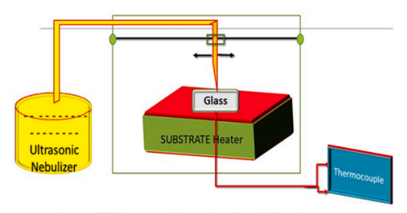
Figure 2:Schematic diagram of ultrasonic spraying system automation setup
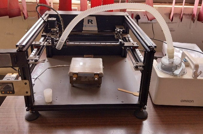
Figure 3: Ultrasonic spray setup
The electrical characteristics thin sheets of CTS are assessed using the Hall Effect technique (Ecopia HMS5000).To simulate sunshine, a 60 milliliters of the MB remedy (1 × 10⁻⁵ M) are illuminated Using a 300 watt halogen light bulb in a photoreactor with two jackets. The MB remedy contains three CTS samples, each measuring 1.5 by 2.5 cm2. For adsorption-desorption to occur Equilibrium, with the films remaining in the mixture in a dark thirty minutes in the environment before being exposed to brightness. Solutions are acquired at predetermined intervals following Light exposure required to operate a UV–vis spectrometer to find the spectra of absorption. The photocatalytic experiment uses a A 300 W fluorescent light illuminates a photoreactor with two jackets containing MB solution in 60 milliliters (1 × 10⁻⁵ M) imitate sunshine. Three 1.5 x 2.5 cm2 CTS samples are inserted into the MB solution. To achieve adsorption-desorption Equilibrium, Films are submerged in the remedy for thirty minutes in a dimly lit area prior to being exposed to light. Solutions are obtained at specific intervals after light irradiation Use a UV-vis spectrometer to identify absorption spectra.
To prevent evaporation of the MB1 solution during chilled water is cycled through the photoreactor with two under light irradiation. Depending on the kind of pyrolysis reaction and nozzle used to spray the solutions, there are many Kinds of SP units. Because the type involving thin films that is produced from SP depends on a number of factors, parameters are important for the development of thin Films. Metal oxide film formations are utilized in many different uses, such as gas sensors, solar cells, optoelectronic devices, supercapacitors, and More, and SP is crucial to their production. To enhance The performance of solar panels, a variety of spray Coating techniques can be used. Here are a few Instances: Photonic smart coatings with Sun Density (PSC): Compared to ordinary cells, this sputtered Nano-optical coating for solar panels’ glass surface Increases the energy yield by 20% by catching more Blue light. Snow-resistant coating: In early tests, this Clear coating reduced the amount of snow and ice that accumulated on solar panels, allowing them to produce Up to 85% more electricity. 234. HYDRASOL: Glass Or polycarbonate solar panels with a self-cleaning, Water-repellent coating technique that makes them hydrophobic.
IV. EXPERIMENTAL RESULTS AND ANALYSIS
The absence of a clear peak. At a lower temperature of substrate, the XRD pattern(T300) indicates the CTS phase is amorphous. It also shown that a substrate temperature higher than that stated during deposition is required for optimal CTS development of thin films. Consequently, no additional T300 characterization is performed besides SEM. It is revealed that when Ts 1 (Ts > 300 °C) rises, The (112) plane becomes more intense, resulting in a significant improvement in Ts > 500 °C. However, when Ts increases, the intensity of the (112) plane decreases, producing weak crystalline films. For the purpose of Producing solar cells, pyrolysis is employed to improve metallic concentration, attain uniform deposition, and Reduce expenses. The atomic 1 % of thin CTS films formed Of chalcogenide at various temperatures (Ts) is determined Using EDX Analysis, and the results are described. Every Sample’s Atomic percentage is determined with a precision Of ±2.EDX data shows that less sulphur was absorbed in The Prepared layer at low temperature (Ts=350°C).
As the temperature rose (Ts>350°C),Re-evaporation from the film’s surface lowered the proportion of Sn atoms, leading to a steady rise in the sulphur reaction rate. In CTS films, the atomic proportion of Cu, Sn, and S reaches the stoichiometric proportion at Ts=500°C (sample T500). As The temperature approaches 550°C, The creation of the SnS2's secondary phase significantly alters the Sn composition (Sn = 25.42).Since sulphur is a volatile element.
Table 1: Bandgap for the CTS films' elemental composition placed at different temperatures
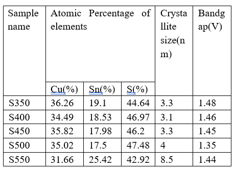
It is discovered that none of the samples contain sulphur. Because Optimizing qualities of CTS thin films in terms of electrical and optical requires managing their constituent composition properties, and films that are out of equilibrium ratio have a significant influence on this.Film made around 20-300°C has been shown to rip off the surface and have adhesion concerns with the substrate. The porous structure is formed in sample T350.Sample T400 displays a flake that resembles a structure. It was discovered that when the temperature Increased, the morphology thin layers of Cu2SnS3 shifted from having a flake-shaped structure to a spherical structure. The sample that is prepared at 500°C is dense and smooth, but when it is heated to 550°C again, porosity is seen in The Film. This could be because a subsequent stage is forming, As seen by the Raman spectrum. All of the deposited thin Films (deposition temperature Ts> 350°C) are present and flawless, with no pinholes or cracks. When comparing the sample generated at 500°C to every other samples, SEM Images showed a compact and flat surface, This is consistent with the XRD results.
Table 2:Characteristics of thin films of CTS electrically at various substrate temperature
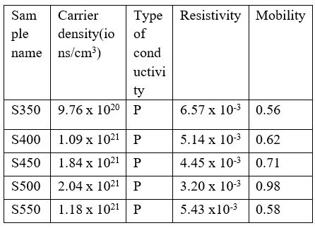
At room temperature, thin films of CTS are electrically tested with a Hall measuring equipment. The table shows the movement and concentration of carriers. Every sample shows p-type conductivity, independent of substrate temperature. CTS films feature high carrier concentrations (1020 to 1021/cm³). The CTS film’s resistivity drops from 6.57×10⁻³ ohm-cm to 3.20×10⁻³ ohm-cm as the temperature rises of the substrate. The CTS Film’s resistivity drops when substrate temperature increases owing to the CTS film’s improved crystallinity. Additionally, several study teams have shown that a rise in crystallite size may be the cause of the reduction in resistivity (apart from T550). (Guo et al.2016). But for the T550 sample, It has been discovered that resistivity rises. This might be brought on by the sample’s high Sn concentration, as shown by EDAX. The sample obtained at Ts=500°C was chosen for further optimisation and analysis, the sample produced at Ts=500°C was selected because to its greater crystallinity, lower resistivity, and higher carrier concentration. Copper concentration’s effect on Cu2SnS3 Thin-film Characteristics. In the thin CTS film precursor solution, The amount of copper is adjusted In sequences between 0.015 M to 0.03 M, or 0.005, while the quantities of Tin and thiourea remain constant at 0.01 M and 0.2 M, Respectively. The base material The temperature is kept at 500 °C, which is the Optimal temperature for this Investigation (Raman etal.2019). CTS1, CTS2, CTS3, and CTS4 are the names of the samples.
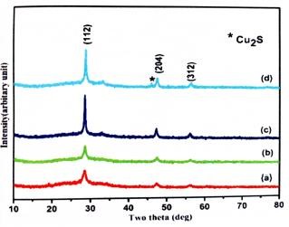
Figure 4: The XRD image of the Cu?SnS3 films
The Cu?SnS3 films' XRD image is displayed in Figure for different copper precursor concentrations. Each sample has peaks at 28.47°, 47.14°, and 56.36°, which match the tetragonal crystal pattern (JCPDS 89-4714) of CTS and correspond to the (112), (204), and (312) planes (Fernandes et al. 2010a). samples S350, S400, S450, S500 shown in figure as a, b, c and d. The three planes present in the prepared samples cause them to be polycrystalline. Additional peaks in sample CTS4 were observed at 46.26°, corresponding to secondary phases of Cu2S.Because of the high concentration of Cu content in the precursor solution, the secondary phase Cu2S formed in CTS4. When the concentration of Cu increases (Cu>0.015M), the intensity of the (112) plane becomes more noticeable, indicating an improvement in the crystallinity of the film. When Cu concentration grows, the Cu signal's strength does as well (Cu>0.025M).
Conclusion
The Cu2SnS3 thin layer was created using inexpensive automated ultrasonic spray pyrolysis procedures, with increments of 50 °C, at various substrate temperatures ranging from 300 °C to 550 °C. Films made at a substrate temperature of 500 °C yield highly crystalline films with a tetragonal Cu2SnS3 phase. Films formed at a higher substrate temperature exhibit the binary phase SnS2. 650.4 nm is found to be the typical thickness of the films. With an order of carrier concentrationthe electrical properties of the films revealed p type conductivity. In regards to thin-film solar cells applications, films from CTS can therefore be employed as a possible absorber layer substance determined by the features.
References
[1] “Temperature dependent growth of Cu2 SnS3 thin films using ultrasonic spray pyrolysis for solar cell absorber layer and photocatalytic application” Sabina Rahaman, Monoj Kumar Singha and Kaustab Ghosh © 2019 IOP Publishing Ltd. [2] “Optimization and fabrication of low cost Cu2SnS3/ZnS thin film heterojunction solar cell using ultrasonic spray pyrolysis” Sabina Rahaman, Monoj Kumar Singha, Kaustab Ghosh Accepted 24 November 20210925-3467/© 2021 Elsevier B.V. [3] “Effect of copper concentration on CTS thin films for solar cell absorber layer and photocatalysis applications” Sabina Rahaman, Monoj Kumar Singha, Kaustab Ghosh Received 2 January 2020; Received in revised form 28 April 2020; Accepted 24 May 2020 0749-6036/© 2020 Elsevier Ltd. [4] “Low-Cost Cu2ZnSnS4 Thin Films for Large-Area High-Efficiency Heterojunction Solar Cells”Sandip Das and Krishna C. Mandal Department of Electrical Engineering, University of South Carolina, Columbia, SC 29208, USA. 978-1-4673-0066-7/12/$26.00 ©2011 IEEE [5] “Fabrication of Spray-Coated Semitransparent Organic Solar Cells” moon hee kang dong kyo heo, da hyun kim, minsu lee, kyungsun ryu,Yong hyun kim, and changhun yun Received 5 September 2019; accepted 20 October 2019. Date of publication 25 October 2019; date of current version 18 November 2019. [6] “Wafer-Bonded GaInP/GaAs//Si Solar Cells With 30% Efficiency Under Concentrated Sunlight” Stephanie Essig, Jan Benick, Michael Schachtner, Alexander Wekkeli, Martin Hermle, and Frank Dimroth, Member, IEEE journal of photovoltaics, vol. 5, no. 3, may 2015. [7] “ZnO Thin Film Deposited by Spray Pyrolysis for Long-Term Stable Organic Solar Cells” Enas Moustafaa, Jose Gb, Lluis F. Marsal, Senior Member, IEEE, and Josep Pallares, Senior Member, IEEE. 2021 IEEE Latin America Electron Devices Conference (LAEDC). April 19-21, 2021.
Copyright
Copyright © 2024 S Pranisha. This is an open access article distributed under the Creative Commons Attribution License, which permits unrestricted use, distribution, and reproduction in any medium, provided the original work is properly cited.

Download Paper
Paper Id : IJRASET64047
Publish Date : 2024-08-22
ISSN : 2321-9653
Publisher Name : IJRASET
DOI Link : Click Here
 Submit Paper Online

