Ijraset Journal For Research in Applied Science and Engineering Technology
- Home / Ijraset
- On This Page
- Abstract
- Introduction
- Conclusion
- References
- Copyright
Probability Driven Double-Edge Triggered Multibit Flip Flop and Clock Gating Integration
Authors: K. Sai Krishna, B. Bhanuprakash, P. Shakthi Ganesh, Dr. D. Sudha
DOI Link: https://doi.org/10.22214/ijraset.2024.61785
Certificate: View Certificate
Abstract
The project delves into the using of Double Edge-Triggered Multi-Bit Flip-Flops (DETMBFFs) alongside Data Driven Clock Gating (DDCG) techniques to bolster power efficiency in digital circuit designs. DETMBFFs enable the data Capture on Both Up and Down Swings of a clock, optimizing throughput while conserving power. By grouping multiple flip-flops and employing a shared clock driver, DETMBFFs minimize redundant clock signals and reduce energy usage. The integration of DDCG selectively disables clock signals based on data activity, further enhancing power efficiency. A novel algorithm, grounded in the ratio of the data to clock toggling and probability-driven grouping of flip-flops within DETMBFFs, is developed to optimize power consumption. Through implementation using Xilinx software tool, the combined approach achieves remarkable power savings ranging from 17% to 23%. This creative approach not only enhances power efficiency but also maintains design integrity, making it a compelling solution for low-power design challenges in digital systems.
Introduction
I. INTRODUCTION
Flip-flops stand as pivotal components in digital systems, serving as key storage units capable of holding binary states, either 0 or 1, with stable 1 and 0 states. These devices possess a unique property of maintaining their current state until prompted to transition by an input signal. Flip-flops are notably sensitive to edge-triggered signals rather than the time or breadth of clock signals[1]. Their versatility extends to various applications including registers, bounce switching removal, frequency division, latches, storing of data, and memory operations.
Among flip-flop types, the Delay flip flop emerges prominently in digital electronics, finding widespread use in the field of shift registers, counters, and input synchronization tasks. The imperative for low-power design arises even in non- portable applications, owing to the escalating energy demands of modern microchips. Traditionally, cooling mechanisms such as fans, large packages and cooling fins have dissipated generated heat.However, with the growing size and density of chips, ensuring adequate cooling has become progressively challenging.
In response to this challenge, efforts to mitigate power consumption now encompass leveraging double edge- triggered flip-flops. These flip-flops, able to record information about edges that are increasing or lowering of clock signals, offer enhanced throughput while conserving power. By consolidating multiple flip-flops and employing a shared clock driver circuit, these DET flip-flops minimize redundant clock signal generation, further optimizing power efficiency.
In Fig 1, grouping a two 1-bit flip-flops to form a 2-bit multi- bit flip-flop (MBFF) showcases this consolidation strategy. Extension of this configuration yields 4-MBFFs, 8- MBFFs, 16-MBFFs, and 32-MBFFs allowing for the representation of an MBFF through the combining of a specific number of individual flip-flops[2]. This method additionally lowers the energy usage attributed to internally present clock drivers but also addresses the problem of power dissipation in modern digital systems. This technique has the involvement of numerous limits and drawbacks that make it inappropriate for most industrial situations, with the exception of a few restricted applications.

The one arithmetic unit, which limiting the pace computing and narrows the control bandwidth, the extreme long delaying in the multi- converter scenario,[3][4] the limited capability to produce non- sequential waves, that are required for non-linear control, the adequate ability to obtain higher performance of the driving signal output and also its degradation with an increase in control channels, and other flaws are some of these.
An other method for contemporary digital power which managing involves utilizing a closed, specialized controller of a particular purpose, like a Voltage Regulator Module (VRM). This approach's limitation to the particular use for which it is developed is a negative. Because a new ASIC design cycle must be started for each case that reports a 15% decrease in the 90-nm processor's total dynamic power, Therefore, using the unit for addressing other power managing issues is not practicable. MBFF characterisation is supported by various tools like cadence liberate.
The advantages of MBFFs are not unpaid. The rate of clock slew is lowered by using common drivers, which causes the clock-to-Q propagation latency to increase and the short-circuit current to rise. One way to increase the MBFF internal clock driver system is to address this, but for the cost of a little bit more power. Therefore, to avert the time closure obstacles brought on through the usage of MBFF during the verilog back-end design phase.
It is advised to implement the MBFF device in the scenario of RTL design because FFs often have very tiny data-to-clock toggling ratios (typically between 0.01 and 0.1).Clock gating isn’t a free service. The clock enabled waves require additional circuitry and interconnects, the accompanying area, power overheads are to be considered. Under the worst situation , an FF's clock inputs can all be turned off separately to obtain the greatest possible clock suppression.
II. LITERATURE SURVEY
- The Ideal Fan-Out of clock Circuit for Adaptive Gating-Based Power Minimization
Clock signal gating is being used more often by the desingers of VLSI chip in an effort to reduce switching power usage.This study delves into probabilistic clock-gating network models to estimate potential energy savings and overheads. By considering process technology and flip-flop toggling probability factors, the minimal fan-out to a clock gated network is determined. Implementing this improved clock gating yields a noteworthy of 10% reduction in overall clock network switching power.[5] The study also discusses the planned implementation of the gating scheme and suggests the idea of combining flip-flops for a unified clocked gating approach.This resulting is consistent with the experimental data which was collected using a 16 bit microcontroller and a 65-nanometer 3- D graphics processor.
2. Power Management of Digital circuit systems For High(efficient) Performance Mixed Signal Systems
THE HPMS platforms demand precise control over different module performances. Creating low-power systems is crucial across various technologies like mobile gadgets and recognition systems, offering benefits even for microcontrollers. Creating low-power gadgets in industrial research contexts presents both challenges and opportunities [6]. This study explores a range of low-energy solutions, including optimizing power-performance trade-offs both in active high and low(standby) states and designing multi- core architectures capable of operating efficiently at lower voltages.
3. Design of seq., circuits using clock gating through driven data
The designing of seq., circuits involves various methodologies. The mbffs are designed by using a low power technique known as LRFF[7].This project focus is on how to implement the combination of two low power design techniques which yields less power dissipation.
4. Double-edge-triggered FFs - IEEE Transactions on computers.
This paper implements the logic double-edge-triggered flipflop in which both positive edge as well as negative edge clock are utilized inorder to obtain precise values of the low power circuits. A det-ff offer potential profits with respect to Speed & energy supply requirements, because there is a chance of occuring fewer redundant logic level changes[8].
III. EXISTING METHODOLOGY
A. Carry-select Adder for Dynamic Power Management
Design of Combinational Logic using Carry-select Adder that yields the optimal toggling correlation. This paper focus involves to find the power savings and also toggling correlations of underlying FFS[9]. In this design, they were used different circuit types such as register files, control units & airthmetic units inorder to find the optimal toggling correlation and also energy savings.
B. Integration of Clock gating circuit with data driven along with multibit flipflops
In this design, initially the clock-gating performs sole opeartion with high power-consumption. The data which driven is introduced to clock gating inorder to get power savings. This resuts in decrease of power consumption by the circuit[10]. But the redundant bits are increased through this circuit. Finally, they eliminated such redundant bits by combining the concept of multibit flipflops with data-driven clock gating circuit which further reduces the power or energy consumption.
C. The Synchronous FIFO logic using mbff with DDCG
The circuit logic rely on the RTL or gate level description. This depends on the methodology of design which this paper follows and it is beyond the scope of this paper [13]. They intoduced synchronous first in first out logic of simple clock gating analysis, such that the results mentioned are not clear , whether they are reducing the power or not.
D. Single Flop-Flop Clock - Gating Driven Through Data Input
At first, in the system level, clock enabling-signals are well defined and can be precisely defined to capture periods where functioning blocks & modules don't require clocking. Those signals are later synthesizable into clock enabling-signals at the gate level automatically. While clock enabling-signals are typically & manually adding for each flip-flop (FF) in the layout process, the state changes of FFs at higher gate levels rely on the basis of type of data that being processed. It's crucial to notedown that the system's dynamic power usage is primarily during periods when module clock signals that are enabled. Implementing data-driven gating incurs area and energy overheads, prompting the proposal to group multiple FFs under the identical clock signal, produced by combining individual enabling signals. However, this approach may reduce disabling effectiveness[11][12].Therefore, it's advantageous to combine the FFs that are with high correlated switching activities and that produce a shared enabling signal.
A recent paper developed asystem for Data-Driven gating based on FF toggling activity, determining the the best clock gate fan-out for maxium power savings. Comprehensive simulations and also statistical observation of FF activity were required inorder to assess the efficacy of clock gating which was data driven since FF state transitions rely on processed data.
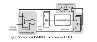
Using clock gating techniquescan decrease dynamic power usage by enabling clock signalsbased on data-driven toggling activity. Gate signals are using to enable flip-flops and latches, with outputs from XOR gates combined through OR logic to produce flip-flops with joint gate -signals and one latch to prevent glitches.
E. Introducing Clock-gating into MBFF
Assume that the probability of data-to-clock toggling is p. Indicate the anticipated energy used by one-bit FF with the symbol(E1).
E1(P)=λ1+µ1p….(1)
where 1µ is energy of given data toggling and 1λ is energy of the inbuilt internal clock driver of the FF. Three alternative outcomes exist for 2-MBFF: neither FF toggles, one FlipFlop toggles, and both FlipFlops toggle. Under the assumption that the data toggling independence, the anticipated energy usage E2 is
E2(p)=(1-p)2+2(λ2+µ2)p(1-p)+(λ2+2µ2)p2 =λ2+2µ2….(2)
where 2µ is the given energy used to toggle each bit of data, and 2λ is energy of the inbuilt internal clock driver. Let x be the one bit data toggling energy and xλ be the MBFFs inbuilt internal clock driver energy for the initial case of x -MBFF. Taking into the consideration of every single possible configuration of flipping FFs, the anticipated energy is
EX(p)=∑j=0 x (λx+jµx)(xj) p j (1-p)xj
=λx+xµx…(3)
One can surely achieve the equivalence in (3) by doing a few 1 rearrangements. The MBFFs which have been covered so far were powered by an ungated clock signal that ran freely. A k- MBFF with a DDCG incorporated is shown as in Fig. 4.1. Every circuit that is darkened is located inside a major cell of a library. ( 2) shown that the equation can be solved for every activity p by finding the group size x that maximises the energy savings[14][15][16].
(1-p)x ln (1-p) CKFF +CKlatch/X 2 =0 …(4)
where the initial clock input load of an FlipFlop and latch, respectively, are denoted by CKFF & CKlatch .
Table 1 displays the answer to equation (4) for a variety of activities, including standard CKFF and CKlatch .
|
P |
0.01 |
0.02 |
0.05 |
0.1 |
|
K |
8 |
6 |
4 |
3 |
Table 1: shows how the ideal MBFF multiplicity varies with toggling probability.
The MBFFs that are covered in the below statements are DDCG unless otherwise indicated. Understanding the energy(power) savings that a x - MBFF can achieve through DDCG, Figure. 3 have been used SPICE to model a range of activities of P and multiplicities 2, 4, 8. The 2-MBFF's power usage. The power used by two individual one-bit FFs given seperatly of each another is shown as blue line (a). The internal clock gating driver at each FF toggles, which is the cause of the 3.8 w power used for zero activity. This power consumption occurs activity independence. Line (b) represents the optimal scenario in which both FFs flip simultaneously.
Toggle the same intial clock driver which is between the 2-FFs or disable it altogether in that case, all thanks to the internal gater shown as in Figure 2.As would be expected, the power used for idle idleness of almost half of the 2 one-bit FFs. Because the gating system uses power in proportion to activity, the power of line (b) increases faster than line (a) when activity increases.Using a 2-MBFF after the 0.17w activity crossing point—the point at which energy starts going off—is useless.
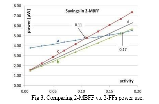
The scenario when the FFs toggles disjointly is depicted in line (c). Given that the driver clock serves both FFs even though only one of them need it, this is clearly the worst scenario. Regarding (b), if the Filp-Flops activities are greater than 0.11, In the stage of disjoint toggling, there cannot be a reason to use two-MBFF. The separation between line (b) or line (c) and line (a) for a certain activity. The 2-MBFF energy savings are shown as in(a). Note that at 0% activity, the power savings per one - bit are (3.8- 1.8)/2=1.0µw.computed the k-MBFF estimated energy savings Epk in an assumption of an ungated, high-zee running μ clock with toggling independence.
Section 3 demonstrated the impact of toggling correlation on the breakeven probability—the point at which an MBFF ceases to save energy. It is obvious that the optimum FF grouping would be those for whichtoggling is nearly entirely connected. It had been demonstrated that the grouping of FFs problem that produces the greatest toggling correlation and, consequently, the greatest energy savings are NP- hard. A workable solution that produces almost the maximum energy savings was published in [10].
The disadvantage of the above method is that, this method necessitates prior understanding of VCD (Value Change Dump) vectors, which are obtained via numerous power simulations that depict the usual functioning and uses of the given design.
Early in the layout process, such data might not be available. The activity given ‘p’ and the MBFFs multiplicity x are combined in the next paragraphs to construct a design flow that minimizes the anticipated wasted energy.The figure which obtained shows how the t w o ( 2 ) -MBFFand f o u r ( 4 ) -MBFF and eight-MBFF, respectively, power savings are put to use. The choice of which MBFF size k best suits an FF, given its activity p, is madeby referring to the interim lines,where Lines (d) in Fig., which depict an MBFF realistic operation, were split by their corresponding multiplicity to get the one-bit power usage. The output is displayed in below Fig. partitions the FF activity range into sections inorder to improve the power savings. The 1-bit ungated FF's power usage is shown by the black line.
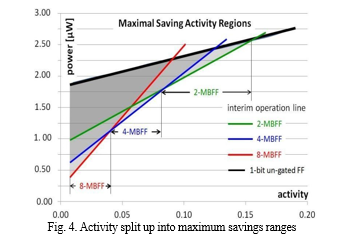
The amount is displayed in the triangle regions delineated by the black and the green line, red, and blue per-bit lines in Figure no:3. splitting up the task into maximum savings ranges produced by grouping an FF of the 2-MBFFs, 4-MBFFs, and 8-MBFFs, respectively, in the terms of power savings per activity. It illustrate that grouping FFs into a 8-MBFF pays out for a low activity. There will come a time when activity surpasses the 8-MBFF and the 4- MBFF yields higher returns. The 2-MBFF outperforms and yields higher returns than the 4-MBFF at higher activities, up to the point where the power(energy) savings terminate. The remaining FFs which are able to classified as un-gated MBFFs to decrement the usage of internal clock (drivers).
We benefit from this behavior and we also gained the best grouping by using the Section III monotonic activity ordering. A suggested MBFFs combining algorithm is as follows.
- Sort the M FFs such that T1 ≤T2 ≤···≤ TN.
- k ← 1.
- Decide on optimal X by Tj , based on Fig above.
- If k > M or X < 2 ( h a l t ) stop.
- Combine FFj, FFj+1,..., FFj+x−1 in a x-MBFF.
- k← k + X.
- Repeat from step 3.
Clock domains shouldn't be crossed by the grouping. The clock enable signals that are manually entered by designers and introduced by RTL synthesis remain unaltered. Groups should examine logical relationships and also pragmatic layout issues..
IV. PROPOSED METHODOLOGY
A. DET- FLIP-FLOP
When a clock initial input changes from 0 to 1, a traditional positive- edge-triggered flip-flops (FF) detects and reacts to the control input or inputs. Changes in the other direction cause it to react absolutely nothing.FFs that are activated by negative edges exhibit comparable behaviour.
Thus the result, these FFs are limited to one response per clock pulse interval. It is suggested that there would be benefits in terms of efficiency and dissipation of energy for DET flip-flops that react to both edges of a clock pulse.[17]
Purpose of DET FF
-
- It allows high data rates.
- We can increase the speed of data transfers
- In registers of microprocessor which has multi-bit FFs.
- SET FF transfer 3 bits per 3 clock pulses.
- But DET FF transfer 6 bits for the similar 3 clock pulses.
Only one clock edge—for example, the positive edge—is consumed by the processor to process information; the negative edge is unemployed for any useful data processing.
We suggest using the below method that had never been done before as in a literature on data centers: double edge clock triggering, in which data is processed using both the positive and negative clock edges. The below equation allows the clock frequency, f, to be cut in half, which will results in an large processor energy savings.
P=Σα*C*V2f.
The secret to putting the above concept into practice is to use Double-Edge-Triggered-Flip-Flops (DET FF), which can operate on both clock edges, rather than the more traditional Single Edge Triggered flip-flops (SET FF). There have been no reports of DET flip-flop usage in any servers' processors[18].
B. Logic Structure of A DET- FLIP-FLOP
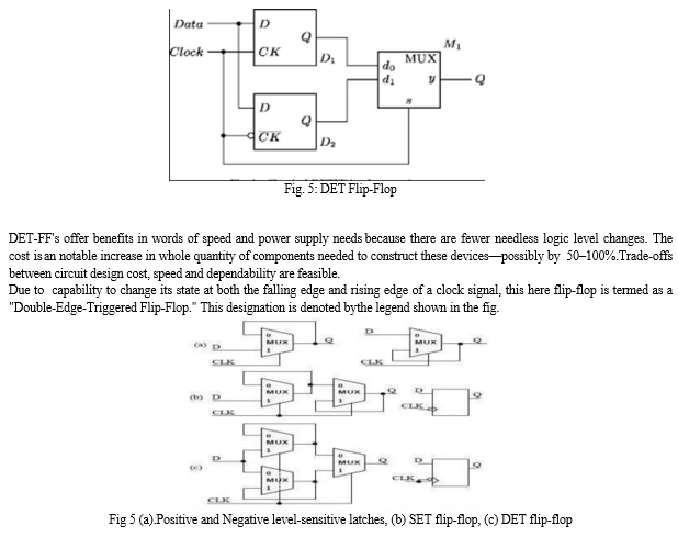
The latch as the basic component for constructing a flip-f structure. It utilizes the levels of a clock signal, CLK, to transition between the storage state and input state. Through the usage of D, Q, and Q' to depict the input signal, current state, and upcoming state of a latch, the state equations for positive and negative level-sensitive latches can be expressed as:
Q' = D.CLK +Q .CLK (1)
Q' = D⋅CLK +Q ⋅CLK (2)
Equation (1) depicts a latch that transfers input data when CLK = 1 and preserves it when CLK = 0. On the contrary, equation (2) illustrates a complementary latch that acquires input data when CLK = 0 and preserves it when CLK = 1. Using a multiplexer (MUX), these logic structures can be constructed.
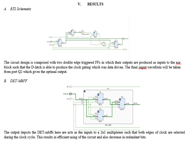
The discussion emphasizes that in an instance of a master latch, no input data is received when CLK = 0. To guarantee the reception of input data at both clock levels, the complementary latches should be linked in parallel instead of in series[19][20]. This configuration results in a "side-by-side flip-flop," as shown. As the flip-flop must remain non-transparent from input to output, it is crucial to always connect the output terminal to the latch in the storage state. Therefore, the MUX indicated by the dotted line becomes essential. With the ability for the flip-flop's state to change during the falling edges and the rising edges of a particular clock pulse, it earns the classification of a "Double-Edge-Triggered Flip-Flop. "In essence, atches act as the fundamental components for flip-flops, transitioning between storage and input states depending on clock signals. When complementary latches are linked in parallel, they formed as a "side-by-side flip-flop," ensuring the lack of transparency from input to output. The term "Double-Edge- Triggered Flip-Flop" indicates its ability to switch states at the edges that are rising and dropping simultaneously of a particular clock signal, emphasizing its significance in digital circuitry.
VI. ACKNOWLEDGMENT
We acknowledge the support provided by Dr. D. Sudha (Associate Professor), J. Seetaram(Assistant Professor), and Dr. E.N.V. Purna Chandra Rao (HOD) for their effort throughout this project.
Conclusion
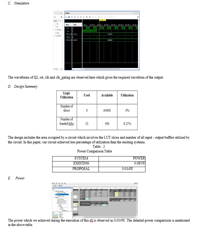
In data stream applications, cutting down power consumption holds evident importance. Utilized widely in sequential circuits, gating of clock and MBFFs serve as pivotal techniques to achieve this objective. Gated clock is instrumental in activating the clock solely during the circuit\'s operation, thereby conserving power during idle times. However, it still leads to creating redundant clock signals. Multi-bit flip-flops aid in decreasing the required no of clock drivers. While comparing to traditional multi-bit flip-flops, considerably more power can be saved by merging flip-flops based on their toggling likelihood. Power efficiency is increased when DET-FFs and clock gating are combined. The utilization of Xilinx software in deploying this strategy ultimately yields substantial power savings propelled by probability-driven DET-MBFFs with clock gating.
References
[1] J. A. bondy & murty, Graph Theory. Srpinger. [2] W.Shen, Hong, & Hu, “Activity & register placement aware gateing clock design,” in 2008. [3] Synopsys design compiler Version E-2011.12-SP2. [4] Strollo and De-caro, “Low-Power FF with clock gated on master & slave latches,” Electron. Lett.pp. 294–295,Feb. 2000. [5] S.Wimer, “On optimal flip-flop grouping for VLSI power minimiza-tion,” Oper. Res. Lett., vol. 41, no. 5, pp.486–489, Sep. 2013 [6] Shmuel Wimer. “On optimal FF grouping for VLSI power(energy) minimization.” Operations Research Letters , no. 5. [7] “A Comparison of Intel’s 32 nm and 22 nm Core i5 CPUs: Power(W), Voltage(V), Temperature(T), and Frequency(F),” Oct. 2012. [8] Yan, Jin Tai, & Zhi Wei Chen. ‘Construction of constrained mbffs for clock power reduction’.In green circuits & systems (ICGCS), International Conference on, IEEE, 2010. [9] A.Farrahi, C.chen, A.srivastava, G.Tellez & M. Sarrafzadeh, ‘Activity driven clock design,’IEEETrans. CAD Integr. Circuits Systems, vol: . 20, No. 6, pp. 705 to 714,Jun. 2001. [10] Dr. S.nirmala & R.praveena, ‘Modified Partial Product bypassing Multiplier for DSP Application,’ International Conference on Innovation in Electronics & Communication Engineering (ICIECE) ,pp. 128, Aug 2013. [11] Power SpyGlass [Online]. Accessible: Early in the process at RTL, the SpyGlass platform gives designers insight into their design using a variety of sophisticated algorithms and analysis tools. For design engineers and managers, it serves as an interactive guiding system that determines the quickest and least expensive way to develop complicated SoCs. [12] Doron Gluzer and Shmuel Wimer, \"Probability Driven Multibit Flip-Flop Integration With Clock Gating,\" in IEEE transactions on VLSI Systems,vol. 25, no. 3, pp. 1173-1177, March 2017. [13] ‘RCA COS/MOS ics,’RCA corp.,1978. [14] S.H.Unger, Asynchronous Sequential circuits. New York : Wiley - Interscience, 1969. [15] J. Hartmanis & R.E.Stearns, Algebraic Structure Theory of Sequential Machines. Englewood Cliffs, NJ : Prentice - Hall, 1966. [16] C. J.Tan, \'Synthesis of asynchronous sequential switching circuits,\" Ph.D. dissertation, Dep. Elec. Eng., Columbia University, New York,1969. [17] C. J. Tan, P. R. Menon, & A. D. Friedman, \"Simplification and decomposition of asynchronous sequential circuits,\" IEEE Trans. Comput.,vol. C-18, pp. 830-838, Sept. 1969. [18] C. E.Stroud, R.R.Munoz, & D. A.pierce, \'Behavioral model Synthesis with Cones,\' IEEE-design test Computation, vol. 5, no. 3, pp. 22–30, Jun. 1988 [19] J. A. Bondy & U.S.R.Murty, Graph Theory : Srpinger, 2008. [20] M. E. Hamid & C. H. Chen \"A Note to Low Power linear f/b shift register\", IEEE Trans. Circuits Syst. II, Analog & Digital Signal Processing, vol. 45, no. 9, pp.1304 -1307 1998.
Copyright
Copyright © 2024 K. Sai Krishna, B. Bhanuprakash, P. Shakthi Ganesh, Dr. D. Sudha. This is an open access article distributed under the Creative Commons Attribution License, which permits unrestricted use, distribution, and reproduction in any medium, provided the original work is properly cited.

Download Paper
Paper Id : IJRASET61785
Publish Date : 2024-05-08
ISSN : 2321-9653
Publisher Name : IJRASET
DOI Link : Click Here
 Submit Paper Online

